AO3404 Specs and Replacement
Type Designator: AO3404
Type of Transistor: MOSFET
Type of Control Channel: N-Channel
Absolute Maximum Ratings
Pd ⓘ - Maximum Power Dissipation: 1.4 W
|Vds|ⓘ - Maximum Drain-Source Voltage: 30 V
|Vgs|ⓘ - Maximum Gate-Source Voltage: 20 V
|Id| ⓘ - Maximum Drain Current: 5 A
Tj ⓘ - Maximum Junction Temperature: 150 °C
Electrical Characteristics
tr ⓘ - Rise Time: 2.5 nS
Cossⓘ - Output Capacitance: 45 pF
RDSonⓘ - Maximum Drain-Source On-State Resistance: 0.031 Ohm
Package: SOT23
AO3404 substitution
- MOSFET ⓘ Cross-Reference Search
AO3404 datasheet
ao3404.pdf
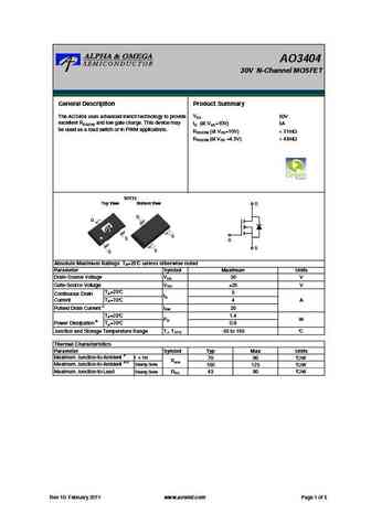
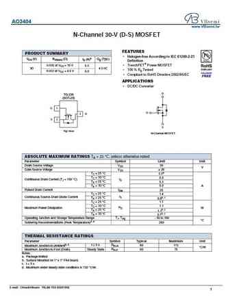
AO3404 30V N-Channel MOSFET General Description Product Summary VDS 30V The AO3404 uses advanced trench technology to provide excellent RDS(ON) and low gate charge. This device may ID (at VGS=10V) 5A be used as a load switch or in PWM applications. RDS(ON) (at VGS=10V) ... See More ⇒
ao3404.pdf
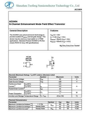
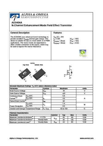
Shenzhen Tuofeng Semiconductor Technology Co., Ltd AO3404 AO3404 N-Channel Enhancement Mode Field Effect Transistor General Description Features The AO3404 uses advanced trench technology to VDS (V) = 30V provide excellent RDS(ON) and low gate charge. This ID = 5.8A (VGS = 10V) device may be used as a load switch or in PWM RDS(ON) ... See More ⇒
ao3404 ko3404.pdf
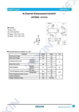
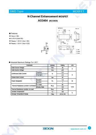
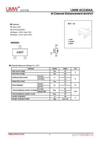
SMD Type IC SMD Type MOSFET N-Channel Enhancement MOSFET AO3404 (KO3404) 3 Features VDS (V) = 30V ID =5.8 A (VGS=10V) 12 RDS(ON) 28 m (VGS =10V) RDS(ON) 43 m (VGS =4.5V) D G S Absolute Maximum Ratings Ta = 25 Parameter Symbol Rating Unit Drain-Source V... See More ⇒
ao3404.pdf
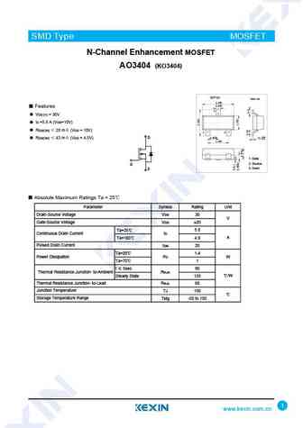
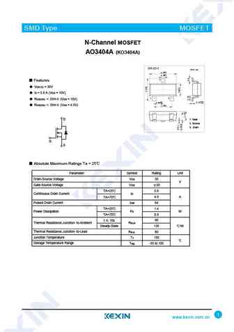
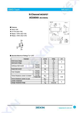
SMD Type IC SMD Type MOSFET N-Channel Enhancement MOSFET AO3404 (KO3404) SOT-23 Unit mm +0.1 2.9 -0.1 +0.1 0.4 -0.1 Features 3 VDS (V) = 30V ID =5.8 A (VGS=10V) RDS(ON) 28 m (VGS = 10V) 1 2 +0.1 +0.05 0.95 -0.1 D 0.1 -0.01 RDS(ON) 43 m (VGS = 4.5V) +0.1 1.9 -0.1 1.Base 1. Gate 2.Emitter 2. Source G 3. Drain 3.collector S Absolute Maximum Ratings Ta = 25 Paramet... See More ⇒
Detailed specifications: MTP9620Q8, MTP9620V8, MTS3572G6, AO3160, AO3162, AO3400A, AO3402, AO3403, IRF520, AO3404A, AO3406, AO3407A, AO3409, AO3413, AO3414, AO3415, AO3415A
Keywords - AO3404 MOSFET specs
AO3404 cross reference
AO3404 equivalent finder
AO3404 pdf lookup
AO3404 substitution
AO3404 replacement
Can't find your MOSFET? Learn how to find a substitute transistor by analyzing voltage, current and package compatibility
History: SI7905DN | AO3403
🌐 : EN ES РУ

LIST
Last Update
MOSFET: AUP060N055 | AUP056N10 | AUP056N08BGL | AUP052N085 | AUP045N12 | AUP039N10 | AUP034N10 | AUP034N06 | AUP033N08BG | AUP026N085
Popular searches
irfz44 datasheet | tip3055 transistor | irf530 datasheet | 2sc2625 | 2sc1815 transistor | 2sd718 | 2n3053 transistor | 2sc458 replacement