APT5017BLC Specs and Replacement
Type Designator: APT5017BLC
Type of Transistor: MOSFET
Type of Control Channel: N-Channel
Absolute Maximum Ratings
Pd ⓘ - Maximum Power Dissipation: 370 W
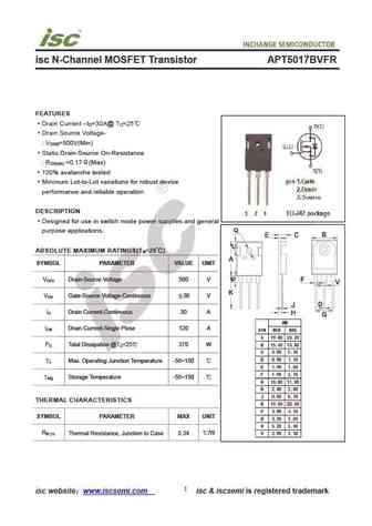
|Vds|ⓘ - Maximum Drain-Source Voltage: 500 V
|Vgs|ⓘ - Maximum Gate-Source Voltage: 30 V
|Id| ⓘ - Maximum Drain Current: 30 A
Tj ⓘ - Maximum Junction Temperature: 150 °C
Electrical Characteristics
tr ⓘ - Rise Time: 15 nS
Cossⓘ - Output Capacitance: 580 pF
RDSonⓘ - Maximum Drain-Source On-State Resistance: 0.17 Ohm
Package: TO247
APT5017BLC substitution
- MOSFET ⓘ Cross-Reference Search
APT5017BLC datasheet
apt5017blc.pdf
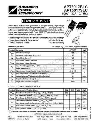
APT5017BLC APT5017SLC 500V 30A 0.170W BLC TM POWER MOS VI D3PAK Power MOS VITM is a new generation of low gate charge, high voltage TO-247 N-Channel enhancement mode power MOSFETs. Lower gate charge is achieved by optimizing the manufacturing process to minimize Ciss and Crss. Lower gate charge coupled with Power MOS VITM optimized gate layout, SLC delivers exceptionally fast switc... See More ⇒
apt5017bvr.pdf
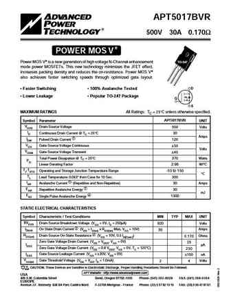
APT5017BVR 500V 30A 0.170 POWER MOS V Power MOS V is a new generation of high voltage N-Channel enhancement TO-247 mode power MOSFETs. This new technology minimizes the JFET effect, increases packing density and reduces the on-resistance. Power MOS V also achieves faster switching speeds through optimized gate layout. D Faster Switching 100% Avalanche Tested Lower ... See More ⇒
apt5017bvfr.pdf
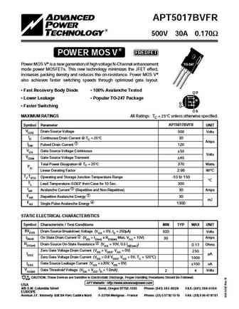
APT5017BVFR 500V 30A 0.170 POWER MOS V FREDFET Power MOS V is a new generation of high voltage N-Channel enhancement TO-247 mode power MOSFETs. This new technology minimizes the JFET effect, increases packing density and reduces the on-resistance. Power MOS V also achieves faster switching speeds through optimized gate layout. Fast Recovery Body Diode 100% Avalanche Test... See More ⇒
apt5017bvr.pdf
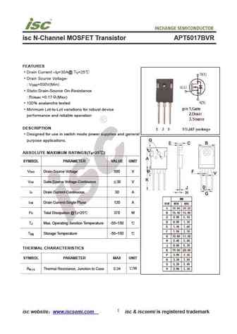
isc N-Channel MOSFET Transistor APT5017BVR FEATURES Drain Current I =30A@ T =25 D C Drain Source Voltage- V =500V(Min) DSS Static Drain-Source On-Resistance R =0.17 (Max) DS(on) 100% avalanche tested Minimum Lot-to-Lot variations for robust device performance and reliable operation DESCRIPTION Designed for use in switch mode power supplies and general purpo... See More ⇒
Detailed specifications: APT5010JLL, APT5010JVRU2, APT5010JVRU3, APT5014B2LC, APT5014BFLL, APT5014BLL, APT5016BFLL, APT5016BLL, P60NF06, APT5018BFLL, APT5018BLL, APT5020BLC, APT5024BFLL, APT5024SVR, APT5027BVR, APT50M50JFLL, APT50M50JLC
Keywords - APT5017BLC MOSFET specs
APT5017BLC cross reference
APT5017BLC equivalent finder
APT5017BLC pdf lookup
APT5017BLC substitution
APT5017BLC replacement
Learn how to find the right MOSFET substitute. A guide to cross-reference, check specs and replace MOSFETs in your circuits.
🌐 : EN ES РУ

LIST
Last Update
MOSFET: FTF30P35D | FTF25N35DHVT | FTF15N35D | FTE15C35G | FTP02P15G | FTE02P15G | AKF30N5P0SX | AKF30N10S | AKF20P45D | CM4407
Popular searches
2sc2166 | 2sc5198 | 2sc1971 | tip41c transistor datasheet | 2n3907 | 12n60 | mp42b transistor | c1675 transistor