SSP2N60B Specs and Replacement
Type Designator: SSP2N60B
Type of Transistor: MOSFET
Type of Control Channel: N-Channel
Absolute Maximum Ratings
Pd ⓘ - Maximum Power Dissipation: 54 W
|Vds|ⓘ - Maximum Drain-Source Voltage: 600 V
|Vgs|ⓘ - Maximum Gate-Source Voltage: 30 V
|Id| ⓘ - Maximum Drain Current: 2 A
Tj ⓘ - Maximum Junction Temperature: 150 °C
Electrical Characteristics
tr ⓘ - Rise Time: 50 nS
Cossⓘ - Output Capacitance: 35 pF
RDSonⓘ - Maximum Drain-Source On-State Resistance: 5 Ohm
Package: TO220
SSP2N60B substitution
- MOSFET ⓘ Cross-Reference Search
SSP2N60B datasheet
ssp2n60b sss2n60b.pdf
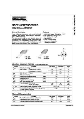
SSP2N60B/SSS2N60B 600V N-Channel MOSFET General Description Features These N-Channel enhancement mode power field effect 2.0A, 600V, RDS(on) = 5.0 @VGS = 10 V transistors are produced using Fairchild s proprietary, Low gate charge ( typical 12.5 nC) planar, DMOS technology. Low Crss ( typical 7.6 pF) This advanced technology has been especially tailored to Fast swit... See More ⇒
ssp2n60a.pdf

Advanced Power MOSFET FEATURES BVDSS = 600 V Avalanche Rugged Technology RDS(on) = 5.0 Rugged Gate Oxide Technology Lower Input Capacitance ID = 2 A Improved Gate Charge Extended Safe Operating Area Lower Leakage Current 25 A (Max.) @ VDS = 600V Lower RDS(ON) 3.892 (Typ.) 1 2 3 1.Gate 2. Drain 3. Source Absolute Maximum Ratings Symbol Characteristic Valu... See More ⇒
ssp2n80a.pdf
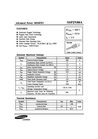
Advanced Power MOSFET FEATURES BVDSS = 800 V Avalanche Rugged Technology RDS(on) = 6.0 Rugged Gate Oxide Technology Lower Input Capacitance ID = 2 A Improved Gate Charge Extended Safe Operating Area Lower Leakage Current 25 A (Max.) @ VDS = 800V Low RDS(ON) 4.688 (Typ.) 1 2 3 1.Gate 2. Drain 3. Source Absolute Maximum Ratings Symbol Characteristic Value Un... See More ⇒
ssp2n90a.pdf

Advanced Power MOSFET FEATURES BVDSS = 900 V Avalanche Rugged Technology RDS(on) = 7.0 Rugged Gate Oxide Technology Lower Input Capacitance ID = 2 A Improved Gate Charge Extended Safe Operating Area Lower Leakage Current 25 A (Max.) @ VDS = 900V Low RDS(ON) 5.838 (Typ.) 1 2 3 1.Gate 2. Drain 3. Source Absolute Maximum Ratings Symbol Characteristic Va... See More ⇒
Detailed specifications: IRFB830, IRFH3205, SI2306, VTI630, VTI630F, VTI634F, VTI640, VTI640F, AON7506, SSS2N60B, 2SK4100LS, 2SK1460, 2SK2010, 2SK1033, 2SK1035, 2SK1036, 2SK1052
Keywords - SSP2N60B MOSFET specs
SSP2N60B cross reference
SSP2N60B equivalent finder
SSP2N60B pdf lookup
SSP2N60B substitution
SSP2N60B replacement
Need a MOSFET replacement? Our guide shows you how to find a perfect substitute by comparing key parameters and specs
History: AP4578GD | 3N75 | BR40P03 | PHB32N06 | SMP40N10 | 2SK388 | 60NM60L-T47
🌐 : EN ES РУ

LIST
Last Update
MOSFET: AUB034N10 | AUB033N08BG | AUB026N085 | AUA062N08BG | AUA060N08AG | AUA056N08BGL | AUA039N10 | ASW80R290E | ASW65R120EFD | ASW65R110E
Popular searches
irf630 datasheet | mpsa13 equivalent | c5198 | 2sc1969 transistor | bcy21 | s8550 datasheet | mj50ac100 | 2sc1318 replacement