2SK2032 Specs and Replacement
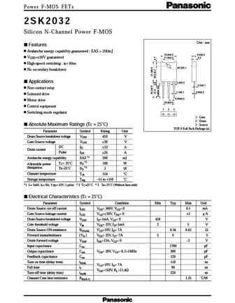
Type Designator: 2SK2032
Type of Transistor: MOSFET
Type of Control Channel: N-Channel
Absolute Maximum Ratings
Pd ⓘ - Maximum Power Dissipation: 100 W
|Vds|ⓘ - Maximum Drain-Source Voltage: 450 V
|Vgs|ⓘ - Maximum Gate-Source Voltage: 30 V
|Id| ⓘ - Maximum Drain Current: 13 A
Tj ⓘ - Maximum Junction Temperature: 150 °C
Electrical Characteristics
Cossⓘ - Output Capacitance: 300 pF
RDSonⓘ - Maximum Drain-Source On-State Resistance: 0.45 Ohm
Package: TOP3
2SK2032 substitution
- MOSFET ⓘ Cross-Reference Search
2SK2032 datasheet
2sk2032.pdf
Power F-MOS FETs 2SK2032 2SK2032 Silicon N-Channel Power F-MOS Unit mm Features Avalanche energy capability guaranteed EAS > 200mJ 15.0 0.3 5.0 0.2 VGSS= 30V guaranteed 11.0 0.2 3.2 High-speed switching tf= 90ns 3.2 0.1 No secondary breakdown Applications 2.0 0.2 2.0 0.1 Non-contact relay 1.1 0.1 0.6 0.2 Solenoid drive 5.45 0.3 Motor drive 10.9 ... See More ⇒
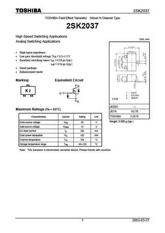
2sk2036.pdf
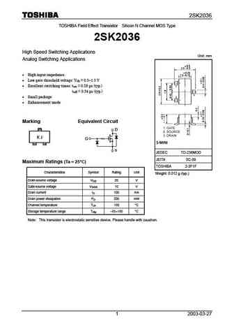
2SK2036 TOSHIBA Field Effect Transistor Silicon N Channel MOS Type 2SK2036 High Speed Switching Applications Unit mm Analog Switching Applications High input impedance. Low gate threshold voltage V = 0.5 1.5 V th Excellent switching times t = 0.28 s (typ.) on t = 0.34 s (typ.) off Small package Enhancement-mode Marking Equivalent Circuit J... See More ⇒
2sk2038.pdf
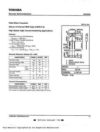
This Material Copyrighted By Its Respective Manufacturer This Material Copyrighted By Its Respective Manufacturer This Material Copyrighted By Its Respective Manufacturer This Material Copyrighted By Its Respective Manufacturer This Material Copyrighted By Its Respective Manufacturer ... See More ⇒
2sk2035.pdf
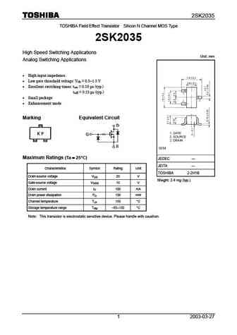
2SK2035 TOSHIBA Field Effect Transistor Silicon N Channel MOS Type 2SK2035 High Speed Switching Applications Unit mm Analog Switching Applications High input impedance. Low gate threshold voltage V = 0.5 1.5 V th Excellent switching times t = 0.16 s (typ.) on t = 0.15 s (typ.) off Small package Enhancement-mode Marking Equivalent Circuit M... See More ⇒
Detailed specifications: 2SK1425, 2SK1426, 2SK1427, 2SJ628, 2SK2011, 2SK2014, 2SK2015, 2SK2016, IRF9540, 2SK2046, 2SK2047, 2SK2074, 2SK2083, 2SK2091, 2SK2101-01MR, 2SK2108, 2SJ616
Keywords - 2SK2032 MOSFET specs
2SK2032 cross reference
2SK2032 equivalent finder
2SK2032 pdf lookup
2SK2032 substitution
2SK2032 replacement
Learn how to find the right MOSFET substitute. A guide to cross-reference, check specs and replace MOSFETs in your circuits.
🌐 : EN ES РУ
LIST
Last Update
MOSFET: ASU70R600E | ASU65R850E | ASU65R550E | ASU65R350E | ASR65R120EFD | ASR65R046EFD | ASQ65R046EFD | ASM65R280E | ASM60R330E | ASE70R950E
Popular searches
a1013 | 2sb554 | 2sd2560 | 2sc2078 transistor | bc558 datasheet | p75nf75 mosfet | ao4407a | mpsa06 datasheet
