2SK1610 Datasheet. Specs and Replacement
Type Designator: 2SK1610 📄📄
Type of Transistor: MOSFET
Type of Control Channel: N-Channel
Absolute Maximum Ratings
Pd ⓘ - Maximum Power Dissipation: 120 W
|Vds|ⓘ - Maximum Drain-Source Voltage: 500 V
|Vgs|ⓘ - Maximum Gate-Source Voltage: 30 V
|Id| ⓘ - Maximum Drain Current: 13 A
Tj ⓘ - Maximum Junction Temperature: 150 °C
Electrical Characteristics
Cossⓘ - Output Capacitance: 300 pF
RDSonⓘ - Maximum Drain-Source On-State Resistance: 0.6 Ohm
Package: SC65
📄📄 Copy
2SK1610 substitution
- MOSFET ⓘ Cross-Reference Search
2SK1610 datasheet
2sk1610.pdf

Power F-MOS FETs 2SK1610 2SK1610 Silicon N-Channel Power F-MOS Unit mm Features 15.0 0.5 4.5 0.2 High avalanche energy capability 13.0 0.5 10.5 0.5 2.0 0.1 VGSS 30V guaranteed Low RDS(on), high-speed switching characteristic 3.2 0.1 Applications High-speed switching (switching mode regulator) 2.0 0.2 For high-frequency power amplification 1.4 0.3 1.1 ... See More ⇒
2sk1610.pdf
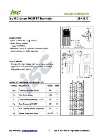
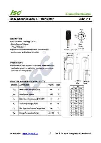
isc N-Channel MOSFET Transistor 2SK1610 DESCRIPTION Drain Current I =13A@ T =25 D C Drain Source Voltage- V =500V(Min) DSS Minimum Lot-to-Lot variations for robust device performance and reliable operation APPLICATIONS Designed for high voltage, high speed power switching applications such as switching regulators, converters, solenoid and relay drivers. ABSOLUTE MAX... See More ⇒
2sk161.pdf
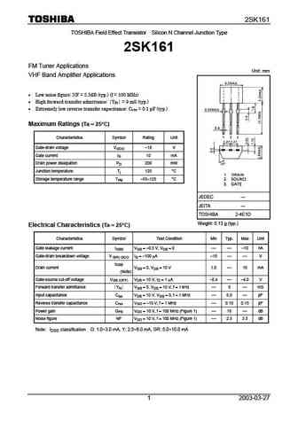
2SK161 TOSHIBA Field Effect Transistor Silicon N Channel Junction Type 2SK161 FM Tuner Applications Unit mm VHF Band Amplifier Applications Low noise figure NF = 2.5dB (typ.) (f = 100 MHz) High forward transfer admittance Y = 9 mS (typ.) fs Extremely low reverse transfer capacitance C = 0.1 pF (typ.) rss Maximum Ratings (Ta = = 25 C) = = Characteris... See More ⇒
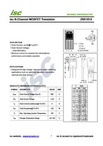
2sk1614.pdf

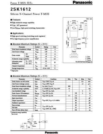
Power F-MOS FETs 2SK1614 2SK1614 Silicon N-Channel Power F-MOS Unit mm Features 15.0 0.5 4.5 0.2 High avalanche energy capability 13.0 0.5 10.5 0.5 2.0 0.1 VGSS, 30V guaranteed Low RDS(on), high-speed switching characteristic 3.2 0.1 Applications High-speed switching (switching mode regulator) 2.0 0.2 For high-frequency power amplification 1.4 0.3 1.1 0... See More ⇒

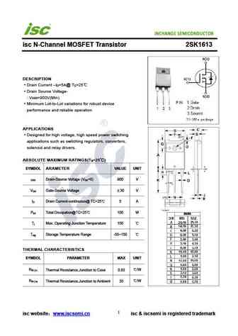
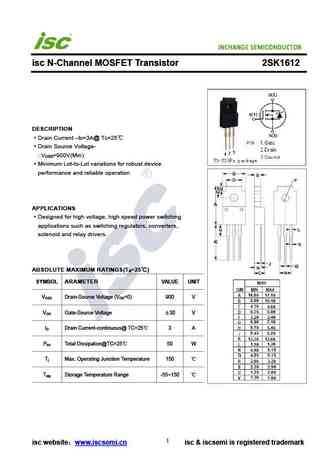
Detailed specifications: 2SJ193, 2SJ194, 2SJ195, 2SK1605, 2SK1606, 2SK1607, 2SK1608, 2SK1609, IRF640, 2SK1612, 2SK1613, 2SK1614, 2SK1724, 2SK1725, 2SK1727, 2SK1728, 2SK1729
Keywords - 2SK1610 MOSFET specs
2SK1610 cross reference
2SK1610 equivalent finder
2SK1610 pdf lookup
2SK1610 substitution
2SK1610 replacement
Step-by-step guide to finding a MOSFET replacement. Cross-reference parts and ensure compatibility for your repair or project.
MOSFET Parameters. How They Affect Each Other
History: APJ14N65D | VBE1202 | IPI80P03P4L-07 | 2SK4057
🌐 : EN ES РУ

LIST
Last Update
MOSFET: CS95118 | CS85105A | CS75N45 | CS72N12 | CS55N50 | CS48N75A | CS40N27 | MSQ60P04D | MSQ40P07D | MSQ30P40D
Popular searches
2sd424 datasheet | 2sc536 datasheet | bd140 transistor equivalent | tip122 transistor equivalent | irfz44n equivalent | 2n2923 | 2n2102 | mj15003g