SSF2307B Specs and Replacement
Type Designator: SSF2307B
Type of Transistor: MOSFET
Type of Control Channel: P-Channel
Absolute Maximum Ratings
Pd ⓘ - Maximum Power Dissipation: 1.25 W
|Vds|ⓘ - Maximum Drain-Source Voltage: 20 V
|Vgs|ⓘ - Maximum Gate-Source Voltage: 12 V
|Id| ⓘ - Maximum Drain Current: 3 A
Tj ⓘ - Maximum Junction Temperature: 150 °C
Electrical Characteristics
tr ⓘ - Rise Time: 8.6 nS
Cossⓘ - Output Capacitance: 210 pF
RDSonⓘ - Maximum Drain-Source On-State Resistance: 0.09 Ohm
Package: SOT23
SSF2307B substitution
- MOSFET ⓘ Cross-Reference Search
SSF2307B datasheet
ssf2307b.pdf
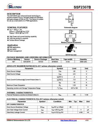
SSF2307B D DESCRIPTION The SSF2307B uses advanced trench technology to provide excellent RDS(ON), low gate charge and operation with gate voltages as low as 2.5V. This device is suitable G for use as a load switch or in PWM applications. S Schematic diagram GENERAL FEATURES VDS = -20V,ID = -3A RDS(ON) ... See More ⇒
ssf2300.pdf
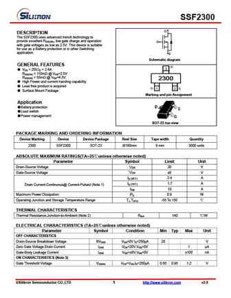
SSF2300 D DESCRIPTION The SSF2300 uses advanced trench technology to provide excellent RDS(ON), low gate charge and operation G with gate voltages as low as 2.5V. This device is suitable for use as a Battery protection or in other Switching application. S Schematic diagram GENERAL FEATURES VDS = 20V,ID = 2.4A RDS(ON) ... See More ⇒
ssf2300a.pdf
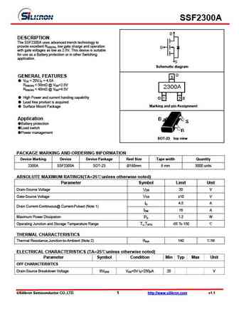
SSF2300A D DESCRIPTION The SSF2300A uses advanced trench technology to provide excellent RDS(ON), low gate charge and operation G with gate voltages as low as 2.5V. This device is suitable for use as a Battery protection or in other Switching application. S Schematic diagram GENERAL FEATURES VDS = 20V,ID = 4.5A RDS(ON) ... See More ⇒
ssf2306.pdf
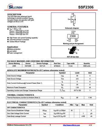
SSF2306 D DESCRIPTION The SSF2306 uses advanced trench technology to provide excellent RDS(ON), G low gate charge and operation with gate voltages as low as 2.5V. S GENERAL FEATURES Schematic diagram VDS = 30V,ID = 5A RDS(ON) ... See More ⇒
Detailed specifications: SSF2300A, SSF2300B, SSF2301, SSF2301A, SSF2301B, SSF2302, SSF2305, SSF2306, AON7408, SSF2312, SSF2314, SSF2316E, SSF2318E, SSF2336, SSF2341E, SSF2356G8, SSF2418E
Keywords - SSF2307B MOSFET specs
SSF2307B cross reference
SSF2307B equivalent finder
SSF2307B pdf lookup
SSF2307B substitution
SSF2307B replacement
Need a MOSFET replacement? Our guide shows you how to find a perfect substitute by comparing key parameters and specs
🌐 : EN ES РУ

LIST
Last Update
MOSFET: FTF30P35D | FTF25N35DHVT | FTF15N35D | FTE15C35G | FTP02P15G | FTE02P15G | AKF30N5P0SX | AKF30N10S | AKF20P45D | CM4407
Popular searches
hy4008 | ncep039n10m | 20n50 | 2sc869 | tip29 transistor equivalent | 2n555 | 2sa564a | c815 transistor