SSF3314E Specs and Replacement
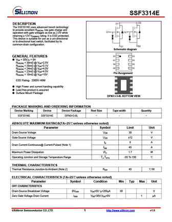
Type Designator: SSF3314E
Type of Transistor: MOSFET
Type of Control Channel: N-Channel
Absolute Maximum Ratings
Pd ⓘ - Maximum Power Dissipation: 1.7 W
|Vds|ⓘ - Maximum Drain-Source Voltage: 30 V
|Vgs|ⓘ - Maximum Gate-Source Voltage: 12 V
|Id| ⓘ - Maximum Drain Current: 8 A
Tj ⓘ - Maximum Junction Temperature: 150 °C
Electrical Characteristics
tr ⓘ - Rise Time: 10 nS
Cossⓘ - Output Capacitance: 130 pF
RDSonⓘ - Maximum Drain-Source On-State Resistance: 0.018 Ohm
Package: DFN3X3-8L
SSF3314E substitution
- MOSFET ⓘ Cross-Reference Search
SSF3314E datasheet
ssf3314e.pdf
SSF3314E DESCRIPTION The SSF3314E uses advanced trench technology to provide excellent RDS(ON), low gate charge and operation with gate voltages as low as 2.5V while retaining a 12V VGS(MAX) rating. It is ESD protected. This device is suitable for use as a uni-directional or bi-directional load switch, facilitated by its common-drain configuration. Schematic diagram GENERAL F... See More ⇒
ssf3341.pdf
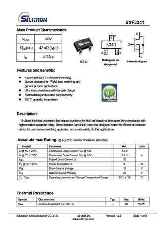
SSF3341 Main Product Characteristics D VDSS -30V G RDS(on) 42m (typ.) S ID -4.2A Marking and pin SOT-23 Schematic diagram Assignme nt Features and Benefits Advanced MOSFET process technology Special designed for PWM, load switching and general purpose applications Ultra low on-resistance with low gate charge Fast switching and reverse body ... See More ⇒
ssf3341l.pdf
SSF3341L D DESCRIPTION The SSF3341L uses advanced trench technology to provide excellent RDS(ON), low gate charge and operation with gate voltages as low as 2.5V. This device is suitable G for use as a load switch or in PWM applications. S GENERAL FEATURES Schematic diagram VDS = -30V,ID = -4.2A RDS(ON) ... See More ⇒
ssf3324.pdf
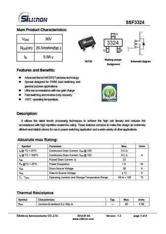
SSF3324 Main Product Characteristics VDSS 30V RDS(on) 26.5mohm(typ.) ID 5.8A Marking and pin SOT23 Schematic diagram Assignme nt Features and Benefits Advanced trench MOSFET process technology Special designed for PWM, load switching and general purpose applications Ultra low on-resistance with low gate charge Fast switching and reverse body rec... See More ⇒
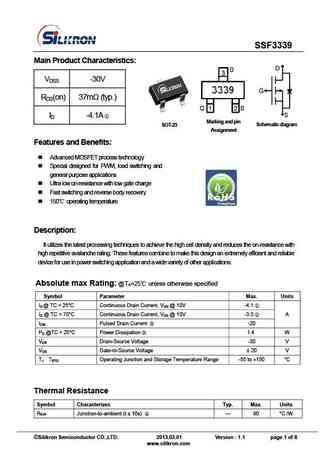
Detailed specifications: SSF3028C1, SSF3036C, SSF3051G7, SSF3055, SSF3056C, SSF3092G1, SSF3117, SSF32E0E, IRFZ24N, SSF3322, SSF3324, SSF3338, SSF3339, SSF3341, SSF3341L, SSF3365, SSF3402
Keywords - SSF3314E MOSFET specs
SSF3314E cross reference
SSF3314E equivalent finder
SSF3314E pdf lookup
SSF3314E substitution
SSF3314E replacement
Need a MOSFET replacement? Our guide shows you how to find a perfect substitute by comparing key parameters and specs
🌐 : EN ES РУ
LIST
Last Update
MOSFET: FTF30P35D | FTF25N35DHVT | FTF15N35D | FTE15C35G | FTP02P15G | FTE02P15G | AKF30N5P0SX | AKF30N10S | AKF20P45D | CM4407
Popular searches
a1023 datasheet | 2sc1080 | 2sb618 | 2sc1328 | 2sc1845 transistor | a933 transistor datasheet | a1633 transistor | 2sa844
