SSF8N65 Specs and Replacement
Type Designator: SSF8N65
Type of Transistor: MOSFET
Type of Control Channel: N-Channel
Absolute Maximum Ratings
Pd ⓘ - Maximum Power Dissipation: 145 W
|Vds|ⓘ - Maximum Drain-Source Voltage: 650 V
|Vgs|ⓘ - Maximum Gate-Source Voltage: 30 V
|Id| ⓘ - Maximum Drain Current: 8.2 A
Tj ⓘ - Maximum Junction Temperature: 150 °C
Electrical Characteristics
tr ⓘ - Rise Time: 78 nS
Cossⓘ - Output Capacitance: 125 pF
RDSonⓘ - Maximum Drain-Source On-State Resistance: 1.2 Ohm
Package: TO220
SSF8N65 substitution
- MOSFET ⓘ Cross-Reference Search
SSF8N65 datasheet
ssf8n65.pdf
SSF8N65 Features VDSS = 650V Extremely high dv/dt capability ID = 8A Low Gate Charge Qg results in Simple Drive Requirement Rdson = 0.95 (typ.) 100% avalanche tested Gate charge minimized Very low intrinsic capacitances Very good manufacturing repeatability Description The SSF8N65 is a new generation of high voltage N Channel enhancement mod... See More ⇒
ssf8n60.pdf

SSF8N60 Features VDSS = 600V Extremely high dv/dt capability ID = 8A Low Gate Charge Qg results in Simple Drive Requirement Rdson = 0.85 (typ.) 100% avalanche tested Gate charge minimized Very low intrinsic capacitances Very good manufacturing repeatability Description The SSF8N60 is a new generation of high voltage N Channel enhancement mod... See More ⇒
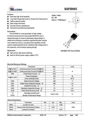
ssf8n80a.pdf
Advanced Power MOSFET FEATURES BVDSS = 800 V Avalanche Rugged Technology RDS(on) = 1.5 Rugged Gate Oxide Technology Lower Input Capacitance ID = 5.5 A Improved Gate Charge Extended Safe Operating Area Lower Leakage Current 25 A (Max.) @ VDS = 800V Low RDS(ON) 1.000 (Typ.) 1 2 3 1.Gate 2. Drain 3. Source Absolute Maximum Ratings Symbol Characteristic Valu... See More ⇒
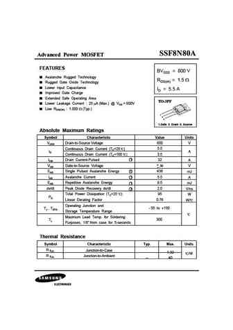
ssf8n90a.pdf
Advanced Power MOSFET FEATURES BVDSS = 900 V Avalanche Rugged Technology RDS(on) = 1.6 Rugged Gate Oxide Technology Lower Input Capacitance ID = 5.5 A Improved Gate Charge Extended Safe Operating Area Lower Leakage Current 25 A (Max.) @ VDS = 900V Low RDS(ON) 1.247 (Typ.) 1 2 3 1.Gate 2. Drain 3. Source Absolute Maximum Ratings Symbol Characteristic Valu... See More ⇒
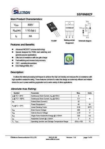
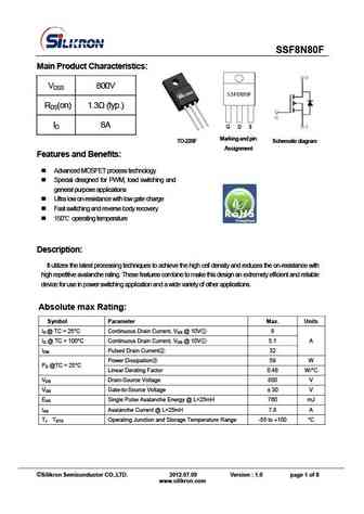
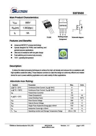
Detailed specifications: SSF8205U, SSF8205UH2, SSF8421, SSF8509, SSF8521, SSF8810, SSF8822, SSF8N60, K3569, SSF8N80, SSF8N80F, SSF8N80ZH, SSF8NP60U, SSF9435, SSF9926, SSF9N90ZH, SSFK3204
Keywords - SSF8N65 MOSFET specs
SSF8N65 cross reference
SSF8N65 equivalent finder
SSF8N65 pdf lookup
SSF8N65 substitution
SSF8N65 replacement
Need a MOSFET replacement? Our guide shows you how to find a perfect substitute by comparing key parameters and specs
