MMFTN501 Specs and Replacement
Type Designator: MMFTN501
Type of Transistor: MOSFET
Type of Control Channel: N-Channel
Absolute Maximum Ratings
Pd ⓘ
- Maximum Power Dissipation: 0.5 W
|Vds|ⓘ - Maximum Drain-Source Voltage: 600 V
|Vgs|ⓘ - Maximum Gate-Source Voltage: 20 V
|Id| ⓘ - Maximum Drain Current: 0.03 A
Tj ⓘ - Maximum Junction Temperature: 150 °C
Electrical Characteristics
tr ⓘ - Rise Time: 55.8 nS
Cossⓘ -
Output Capacitance: 4.53 pF
RDSonⓘ - Maximum Drain-Source On-State Resistance: 700 Ohm
Package: TO236
- MOSFET ⓘ Cross-Reference Search
MMFTN501 datasheet
..1. Size:216K semtech
mmftn501.pdf 

MMFTN501 Silicon N-Channel MOSFET 1. Gate 2. Source 3. Drain TO-236 Plastic Package Drain Gate Source Absolute Maximum Ratings (Ta = 25 unless otherwise specified) Parameter Symbol Value Unit Drain-Source Voltage VDSX 600 V Gate-Source Voltage VGSS 20 V 30 mA Drain Current ID Peak Drain Current1) IDM 120 mA Maximum Continuous Source Current IS 25 mA Maximum Pulse So... See More ⇒
9.1. Size:522K semtech
mmftn3019e.pdf
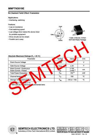
MMFTN3019E N-Channel Field Effect Transistor Applications Interfacing, switching Features Drain Low on-resistance Fast switching speed Low voltage drive makes this device ideal for portable equipment Gate Drive circuits can be simple Parallel use is easy Source O Absolute Maximum Ratings (Ta = 25 C) Parameter Symbol Value Unit Drain-Source Vo... See More ⇒
9.2. Size:154K semtech
mmftn20.pdf
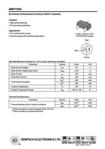
MMFTN20 N-Channel Enhancement Vertical D-MOS Transistor Features High-speed switching No secondary breakdown Applications Thin and thick film circuits 1. Gate 2. Source 3. Drain General purpose fast switching applications TO-236 Plastic Package Drain Gate Source O Absolute Maximum Ratings (Ta = 25 C unless otherwise specified) Parameter Symbol Value Unit ... See More ⇒
9.3. Size:154K semtech
mmftn138.pdf
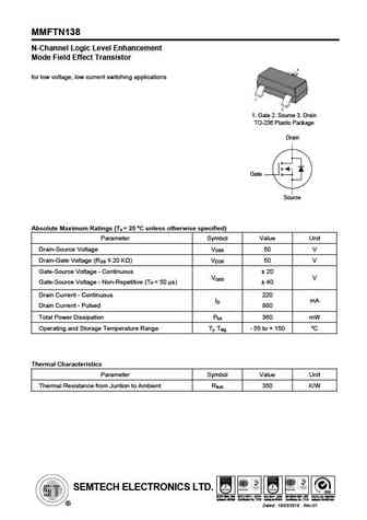
MMFTN138 N-Channel Logic Level Enhancement Mode Field Effect Transistor for low voltage, low current switching applications 1. Gate 2. Source 3. Drain TO-236 Plastic Package Drain Gate Source O Absolute Maximum Ratings (Ta = 25 C unless otherwise specified) Parameter Symbol Value Unit Drain-Source Voltage VDSS 50 V Drain-Gate Voltage (RGS 20 K ) VDGR 50 V Gate-Source ... See More ⇒
9.4. Size:215K semtech
mmftn3406.pdf
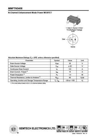
MMFTN3406 N-Channel Enhancement Mode Power MOSFET 1. Gate 2. Source 3. Drain TO-236 Plastic Package Drain Gate Source Absolute Maximum Ratings (Ta = 25 unless otherwise specified) Parameter Symbol Value Unit Drain-Source Voltage VDSS 30 V Gate-Source Voltage VGS 20 V Continuous Drain Current ID 3.6 A Drain Current - Pulsed 1) IDM 15 A Power Dissipation 1) Pd 1.4 W Therm... See More ⇒
9.5. Size:462K semtech
mmftn3018w.pdf
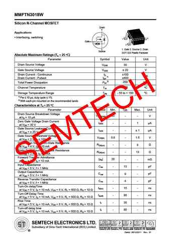
MMFTN3018W Silicon N-Channel MOSFET Drain Applications Interfacing, switching Gate 1. Gate 2. Source 3. Drain Source SOT-323 Plastic Package O Absolute Maximum Ratings (Ta = 25 C) Parameter Symbol Value Unit Drain Source Voltage VDSS 30 V Gate Source Voltage VGSS 20 V Drain Current - Continuous ID 100 mA Drain Current - Pulsed IDP 1) 400 200 mW Total Power ... See More ⇒
9.6. Size:910K semtech
mmftn138w.pdf
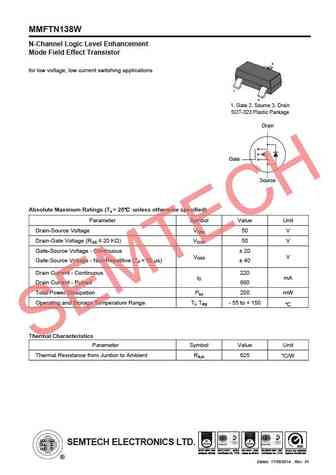
MMFTN138W N-Channel Logic Level Enhancement Mode Field Effect Transistor for low voltage, low current switching applications 1. Gate 2. Source 3. Drain SOT-323 Plastic Package Drain Gate Source Absolute Maximum Ratings (Ta = 25 unless otherwise specified) Parameter Symbol Value Unit Drain-Source Voltage VDSS 50 V Drain-Gate Voltage (RGS 20 K ) VDGR 50 V Gate-Source V... See More ⇒
9.7. Size:153K semtech
mmftn123.pdf
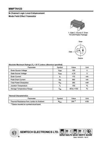
MMFTN123 N-Channel Logic Level Enhancement Mode Field Effect Transistor 1. Gate 2. Source 3. Drain TO-236 Plastic Package Drain Gate Source O Absolute Maximum Ratings (Ta = 25 C unless otherwise specified) Parameter Symbol Value Unit Drain-Source Voltage VDSS 100 V Gate-Source Voltage VGSS 20 V Drain Current ID 170 mA Peak Drain Current IDM 680 mA Total Power Dissipation P... See More ⇒
9.8. Size:236K semtech
mmftn2306.pdf
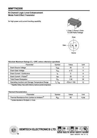
MMFTN2306 N-Channel Logic Level Enhancement Mode Field Effect Transistor for high power and current handing capability 1. Gate 2. Source 3. Drain TO-236 Plastic Package Drain Gate Source Absolute Maximum Ratings (Ta = 25 unless otherwise specified) Parameter Symbol Value Unit Drain-Source Voltage VDSS 30 V Drain-Gate Voltage VGS 12 V Drain Current - Continuous ID 5 A ... See More ⇒
9.9. Size:114K semtech
mmftn170.pdf
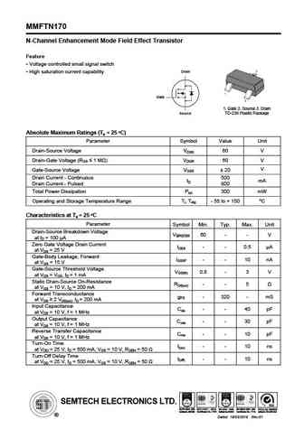
MMFTN170 N-Channel Enhancement Mode Field Effect Transistor Feature Voltage controlled small signal switch Drain High saturation current capability Gate 1. Gate 2. Source 3. Drain Source TO-236 Plastic Package O Absolute Maximum Ratings (Ta = 25 C) Parameter Symbol Value Unit Drain-Source Voltage VDSS 60 V Drain-Gate Voltage (RGS 1 M ) VDGR 60 V V Gate-Source... See More ⇒
9.10. Size:377K semtech
mmftn2302.pdf
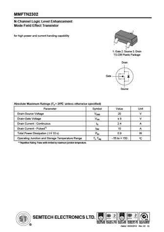
MMFTN2302 N-Channel Logic Level Enhancement Mode Field Effect Transistor for high power and current handing capability 1. Gate 2. Source 3. Drain TO-236 Plastic Package Drain Gate Source Absolute Maximum Ratings (Ta = 25 unless otherwise specified) Parameter Symbol Value Unit Drain-Source Voltage VDSS 20 V Drain-Gate Voltage VGS 8 V Drain Current - Continuous ID 2.4 A ... See More ⇒
9.11. Size:640K semtech
mmftn290e.pdf
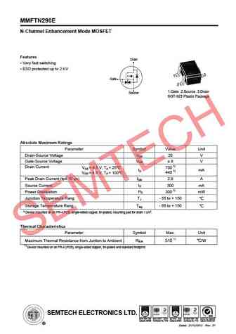
MMFTN290E N-Channel Enhancement Mode MOSFET Features Drain Very fast switching ESD protected up to 2 KV Gate Source Absolute Maximum Ratings Parameter Symbol Value Unit Drain-Source Voltage VDS 20 V Gate-Source Voltage VGS 8 V Drain Current VGS = 4.5 V, TA = 25 700 1) ID mA 440 1) VGS = 4.5 V, TA = 100 Peak Drain Current (tp 10 s) IDM 2.8 A S... See More ⇒
9.12. Size:330K msksemi
mmftn3019e-ms.pdf
www.msksemi.com MMFTN3019E-MS Semiconductor Compiance Absolute Maximum Ratings T = 25 C unless otherwise noted A Symbol Parameter Value Units VDS Drain-Source Voltage 30 V VGS Continuous Gate-Source Voltage 20V V 3 I Continuous Drain Current 100 mA D P Power Dissipation 150 mW D 2 R JA Thermal Resistance from Junction to Ambient 833 C /W 1. Gate 2. Source TSTG Storage Te... See More ⇒
9.13. Size:889K cn vbsemi
mmftn170.pdf
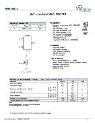
MMFTN170 www.VBsemi.tw N-Channel 60-V (D-S) MOSFET FEATURES PRODUCT SUMMARY Halogen-free According to IEC 61249-2-21 VDS (V) RDS(on) ( )ID (mA) Definition 2.8 at VGS = 10 V 60 250 Low Threshold 2 V (typ.) Low Input Capacitance 25 pF Fast Switching Speed 25 ns Low Input and Output Leakage SOT-23 TrenchFET Power MOSFET 1200V ESD Protection G 1 ... See More ⇒
Detailed specifications: MMFTN170, MMFTN20, MMFTN2302, MMFTN2306, MMFTN290E, MMFTN3018W, MMFTN3019E, MMFTN3406, 20N60, MMFTP84W, ST2N7000, MMFTN138W, 2SK2876-01MR, 2SK1356, SD211DE, SD213DE, SD215DE
Keywords - MMFTN501 MOSFET specs
MMFTN501 cross reference
MMFTN501 equivalent finder
MMFTN501 pdf lookup
MMFTN501 substitution
MMFTN501 replacement
Learn how to find the right MOSFET substitute. A guide to cross-reference, check specs and replace MOSFETs in your circuits.
