PK650BA Datasheet. Specs and Replacement
Type Designator: PK650BA 📄📄
Type of Transistor: MOSFET
Type of Control Channel: N-Channel
Absolute Maximum Ratings
Pd ⓘ - Maximum Power Dissipation: 31 W
|Vds|ⓘ - Maximum Drain-Source Voltage: 30 V
|Vgs|ⓘ - Maximum Gate-Source Voltage: 20 V
|Id| ⓘ - Maximum Drain Current: 70 A
Tj ⓘ - Maximum Junction Temperature: 150 °C
Electrical Characteristics
tr ⓘ - Rise Time: 10 nS
Cossⓘ - Output Capacitance: 311 pF
RDSonⓘ - Maximum Drain-Source On-State Resistance: 0.0033 Ohm
Package: PDFN5X6P
📄📄 Copy
PK650BA substitution
- MOSFET ⓘ Cross-Reference Search
PK650BA datasheet
pk650ba.pdf
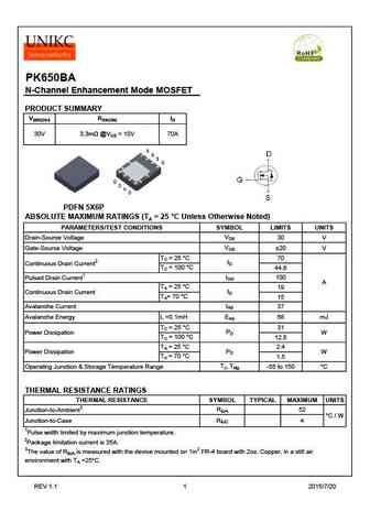
PK650BA N-Channel Enhancement Mode MOSFET PRODUCT SUMMARY V(BR)DSS RDS(ON) ID 3.3m @VGS = 10V 30V 70A PDFN 5X6P ABSOLUTE MAXIMUM RATINGS (TA = 25 C Unless Otherwise Noted) PARAMETERS/TEST CONDITIONS SYMBOL LIMITS UNITS VDS Drain-Source Voltage 30 V VGS Gate-Source Voltage 20 V TC = 25 C 70 ID Continuous Drain Current2 TC = 100 C 44.6 IDM 100 Pulsed Drain Cur... See More ⇒
pk650ba.pdf
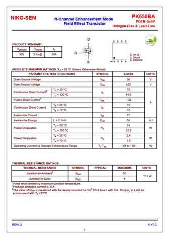
PK650BA NIKO-SEM N-Channel Enhancement Mode PDFN 5x6P Field Effect Transistor Halogen-Free & Lead-Free D D D D D PRODUCT SUMMARY V(BR)DSS RDS(ON) ID G 30V 3.3m 70A G. GATE D. DRAIN S. SOURCE #1 S S S G S ABSOLUTE MAXIMUM RATINGS (TA = 25 C Unless Otherwise Noted) PARAMETERS/TEST CONDITIONS SYMBOL LIMITS UNITS Drain-Source Voltage VDS 30 V Gate-Source Vol... See More ⇒
pk650dy.pdf
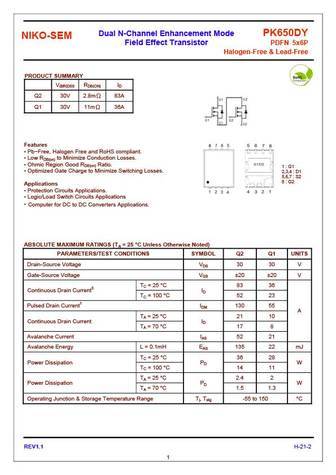
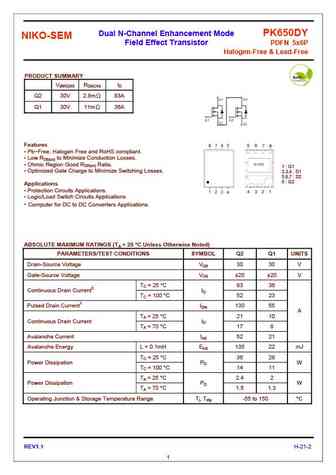
Dual N-Channel Enhancement Mode PK650DY NIKO-SEM Field Effect Transistor PDFN 5x6P Halogen-Free & Lead-Free PRODUCT SUMMARY V(BR)DSS RDS(ON) ID Q2 30V 2.8m 83A Q1 30V 11m 36A Features Pb-Free, Halogen Free and RoHS compliant. Low RDS(on) to Minimize Conduction Losses. Ohmic Region Good RDS(on) Ratio. 1 G1 Optimized Gate Charge to Minimize Switch... See More ⇒
pk650dy.pdf
Dual N-Channel Enhancement Mode PK650DY NIKO-SEM Field Effect Transistor PDFN 5x6P Halogen-Free & Lead-Free PRODUCT SUMMARY V(BR)DSS RDS(ON) ID Q2 30V 2.8m 83A Q1 30V 11m 36A Features Pb-Free, Halogen Free and RoHS compliant. Low RDS(on) to Minimize Conduction Losses. Ohmic Region Good RDS(on) Ratio. 1 G1 Optimized Gate Charge to Minimize Switch... See More ⇒
Detailed specifications: PK612DZ, PK615BM6, PK615BMA, PK616BA, PK618BA, PK626BA, PK632BA, PK636BA, SI2302, PK664BA, PK696BA, PK698SA, PK6A6BA, PK6B2BA, PK6H2BA, PA002FMA, PA002FMG
Keywords - PK650BA MOSFET specs
PK650BA cross reference
PK650BA equivalent finder
PK650BA pdf lookup
PK650BA substitution
PK650BA replacement
Can't find your MOSFET? Learn how to find a substitute transistor by analyzing voltage, current and package compatibility
