PK5G6EA Datasheet. Specs and Replacement
Type Designator: PK5G6EA 📄📄
Type of Transistor: MOSFET
Type of Control Channel: N-Channel
Absolute Maximum Ratings
Pd ⓘ - Maximum Power Dissipation: 31 W
|Vds|ⓘ - Maximum Drain-Source Voltage: 20 V
|Vgs|ⓘ - Maximum Gate-Source Voltage: 12 V
|Id| ⓘ - Maximum Drain Current: 87 A
Tj ⓘ - Maximum Junction Temperature: 150 °C
Electrical Characteristics
tr ⓘ - Rise Time: 58 nS
Cossⓘ - Output Capacitance: 659 pF
RDSonⓘ - Maximum Drain-Source On-State Resistance: 0.0024 Ohm
Package: PDFN5X6P
📄📄 Copy
PK5G6EA substitution
- MOSFET ⓘ Cross-Reference Search
PK5G6EA datasheet
pk5g6ea.pdf
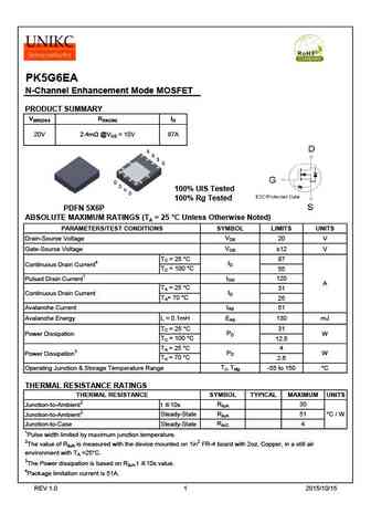
PK5G6EA N-Channel Enhancement Mode MOSFET PRODUCT SUMMARY V(BR)DSS RDS(ON) ID 2.4m @VGS = 10V 20V 87A 100% UIS Tested 100% Rg Tested PDFN 5X6P ABSOLUTE MAXIMUM RATINGS (TA = 25 C Unless Otherwise Noted) PARAMETERS/TEST CONDITIONS SYMBOL LIMITS UNITS VDS Drain-Source Voltage 20 V VGS Gate-Source Voltage 12 V TC = 25 C 87 ID Continuous Drain Current4 TC = 100 C ... See More ⇒
pk5g6ea.pdf
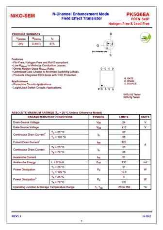
N-Channel Enhancement Mode PK5G6EA NIKO-SEM Field Effect Transistor PDFN 5x6P Halogen-Free & Lead-Free PRODUCT SUMMARY V(BR)DSS RDS(ON) ID 2.4m 24V 87A ESD Protected Gate Features Pb-Free, Halogen Free and RoHS compliant. Low RDS(on) to Minimize Conduction Losses. D D D D Ohmic Region Good RDS(on) Ratio. Optimized Gate Charge to Minimize Switching ... See More ⇒
Detailed specifications: PA610NV, PB5A2BA, PB5G2JU, PE5A0DZ, PE5A1BA, PE5G6EA, PK5A1BA, PK5C8EA, IRF640, PB210BC, PB210BD, PB210BI, PB210BM, PB210BTF, PB210BV, PB210HV, PK510BA
Keywords - PK5G6EA MOSFET specs
PK5G6EA cross reference
PK5G6EA equivalent finder
PK5G6EA pdf lookup
PK5G6EA substitution
PK5G6EA replacement
Can't find your MOSFET? Learn how to find a substitute transistor by analyzing voltage, current and package compatibility
History: IXTT75N10L2
🌐 : EN ES РУ

LIST
Last Update
MOSFET: BCD70N07A | BCD90N03 | BCD80N06 | T50N06 | H50N06 | BCD12N65 | BCT12N65 | BCD4N65 | BCT4N65 | BCD7N65
Popular searches
2sc1913 | c2314 transistor | c2482 transistor | 2sc1222 replacement | 2sa725 | c5242 transistor | 2sa726 replacement | a1941 datasheet