All MOSFET. APM7313K Datasheet


APM7313K MOSFET. Datasheet pdf. Equivalent


   Type Designator: APM7313K
   Type of Transistor: MOSFET
   Type of Control Channel: N -Channel
   Pdⓘ - Maximum Power Dissipation: 2 W
   |Vds|ⓘ - Maximum Drain-Source Voltage: 30 V
   |Vgs|ⓘ - Maximum Gate-Source Voltage: 20 V
   |Vgs(th)|ⓘ - Maximum Gate-Threshold Voltage: 2 V
   |Id|ⓘ - Maximum Drain Current: 6 A
   Tjⓘ - Maximum Junction Temperature: 150 °C
   Qgⓘ - Total Gate Charge: 19 nC
   trⓘ - Rise Time: 8 nS
   Cossⓘ - Output Capacitance: 150 pF
   Rdsⓘ - Maximum Drain-Source On-State Resistance: 0.028 Ohm
   Package: SOP8

 APM7313K Transistor Equivalent Substitute - MOSFET Cross-Reference Search


APM7313K Datasheet (PDF)

 ..1. Size:192K  anpec
apm7313k.pdf

APM7313K APM7313K

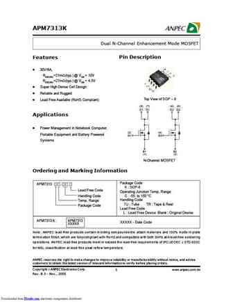
APM7313KDual N-Channel Enhancement Mode MOSFETPin DescriptionFeatures 30V/6A,RDS(ON) =21m(typ.) @ VGS = 10VRDS(ON) =27m(typ.) @ VGS = 4.5V Super High Dense Cell Design Reliable and RuggedTop View of SOP - 8 Lead Free Available (RoHS Compliant)(8) (7) (6) (5)D1 D1 D2 D2Applications Power Management in Notebook Computer,(2) (4)Portable Equipment and Battery P

 0.1. Size:835K  cn vbsemi
apm7313kc.pdf

APM7313K APM7313K

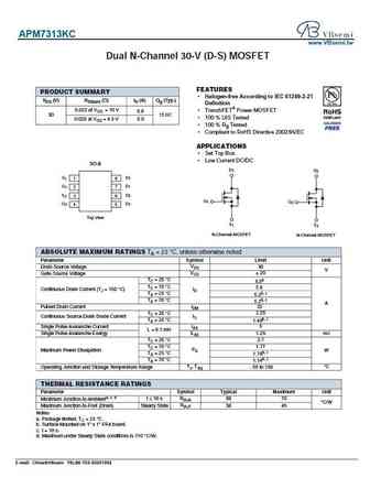
APM7313KCwww.VBsemi.twDual N-Channel 30-V (D-S) MOSFETFEATURESPRODUCT SUMMARY Halogen-free According to IEC 61249-2-21VDS (V) RDS(on) ()ID (A) Qg (Typ.)Definition0.022 at VGS = 10 V TrenchFET Power MOSFET6.830 15 nC 100 % UIS Tested0.026 at VGS = 4.5 V 6.0 100 % Rg Tested Compliant to RoHS Directive 2002/95/ECAPPLICATIONS Set Top Box

 8.1. Size:216K  anpec
apm7318.pdf

APM7313K APM7313K

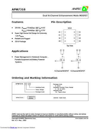
APM7318Dual N-Channel Enhancement Mode MOSFETFeatures Pin Description 20V/8A , RDS(ON)=15m(typ.) @ VGS=4.5VSO-8RDS(ON)=30m(typ.) @ VGS=2.5VS1 1 8 D1 Super High Dense Cell Design for ExtremelyG1 2 7 D1Low RDS(ON)S2 3 6 D2 Reliable and RuggedG2 45 D2 SO-8 PackageTop ViewD1 D1 D2 D2Applica

 8.2. Size:139K  anpec
apm7312k.pdf

APM7313K APM7313K

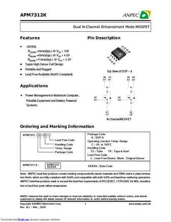
APM7312KDual N-Channel Enhancement Mode MOSFETFeatures Pin DescriptionD1 20V/6A,D1D2RDS(ON) =35m(typ.) @ VGS = 10VD2 RDS(ON) =45m(typ.) @ VGS = 4.5VS1 G1 RDS(ON) =110m(typ.) @ VGS = 2.5VS2G2 Super High Dense Cell Design Reliable and Rugged Top View of SOP - 8 Lead Free Available (RoHS Compliant)

 8.3. Size:137K  anpec
apm7314k.pdf

APM7313K APM7313K

APM7314KDual N-Channel Enhancement Mode MOSFETFeatures Pin DescriptionD1 30V/8A,D1D2RDS(ON) =18m(typ.) @ VGS = 10VD2 RDS(ON) =23m(typ.) @ VGS = 4.5VS1G1 Super High Dense Cell DesignS2G2 Reliable and RuggedTop View of SOP - 8 Lead Free Available (RoHS Compliant)(8) (7) (6) (5)D1 D1

 8.4. Size:142K  anpec
apm7318k.pdf

APM7313K APM7313K

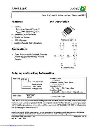
APM7318KDual N-Channel Enhancement Mode MOSFETFeatures Pin DescriptionD1 20V/8A,D1D2RDS(ON) =15m(typ.) @ VGS =4.5VD2 RDS(ON) =30m(typ.) @ VGS =2.5VS1G1 Super High Dense Cell DesignS2G2 Reliable and RuggedTop View of SOP - 8 SOP-8 Package Lead Free Available (RoHS Compliant)

 8.5. Size:161K  anpec
apm7316.pdf

APM7313K APM7313K

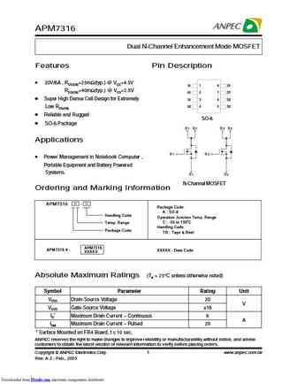
APM7316Dual N-Channel Enhancement Mode MOSFETFeatures Pin Description 20V/6A , RDS(ON)=25m(typ.) @ VGS=4.5VS1 1 8 D1RDS(ON)=40m(typ.) @ VGS=2.5VG1 2 7 D1 Super High Dense Cell Design for ExtremelyS2 3 6 D2G2 4 5 D2Low RDS(ON) Reliable and RuggedSO-8 SO-8 PackageD1 D1 D2 D2ApplicationsG1

 8.6. Size:178K  anpec
apm7314.pdf

APM7313K APM7313K

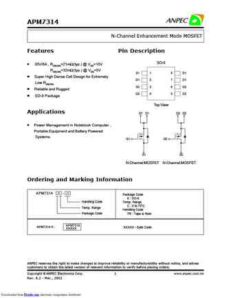
APM7314N-Channel Enhancement Mode MOSFETFeatures Pin DescriptionSO-8 30V/6A , RDS(ON)=21m(typ.) @ VGS=10VRDS(ON)=32m(typ.) @ VGS=5VS1 1 8 D1 Super High Dense Cell Design for ExtremelyG1 2 7 D1Low RDS(ON)S2 3 6 D2 Reliable and RuggedG2 45 D2 SO-8 PackageTop ViewApplicationsD1 D1 D2 D2

 8.7. Size:146K  anpec
apm7312.pdf

APM7313K APM7313K

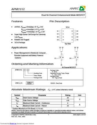
APM7312 Dual N-Channel Enhancement Mode MOSFETFeatures Pin Description 20V/6A , RDS(ON)=35m(typ.) @ VGS=10VSO-8RDS(ON)=45m(typ.) @ VGS=4.5VS1 1 8 D1 RDS(ON)=110m(typ.) @ VGS=2.5VG1 2 7 D1 Super High Dense Cell Design for ExtremelyS2 3 6 D2Low RDS(ON) Reliable and Rugged G2 45 D2 SO-8 Package

 8.8. Size:1469K  cn vbsemi
apm7318kc.pdf

APM7313K APM7313K

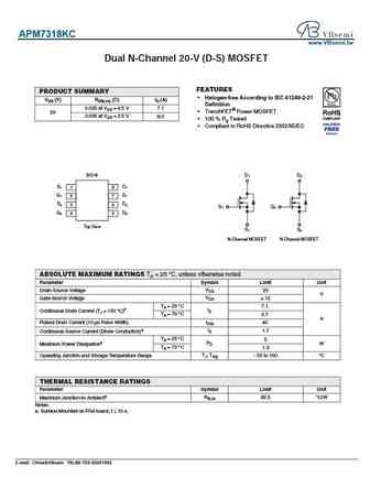
APM7318KCwww.VBsemi.twDual N-Channel 20-V (D-S) MOSFETFEATURESPRODUCT SUMMARY Halogen-free According to IEC 61249-2-21VDS (V) RDS(on) ()ID (A)Definition0.025 at VGS = 4.5 V 7.1 TrenchFET Power MOSFET200.035 at VGS = 2.5 V 6.0 100 % Rg Tested Compliant to RoHS Directive 2002/95/ECSO-8 D1 D2S1 1 D18G1 2 D17S2 3 D26G1 G2G2 4 D25

Datasheet: FMM50-025TF , FMM60-02TF , FMM75-01F , FMP26-02P , FMP36-015P , FMP76-01T , GMM3x100-01X1-SMD , FDMS0306AS , RFP50N06 , FDMS0300S , GMM3x160-0055X2-SMD , FDMC7200S , GMM3x180-004X2-SMD , FDMC7200 , GMM3x60-015X2-SMD , FDMC0310AS , GWM100-0085X1-SL .

History: 2SK4014 | FDS6685 | DMN4031SSD | NCEP045N10AG | FDS8949F085 | FDS9934C | JCS2N95RA


Back to Top