2026 Specs and Replacement
Type Designator: 2026
Type of Transistor: MOSFET
Type of Control Channel: P-Channel
Absolute Maximum Ratings
Pd ⓘ
- Maximum Power Dissipation: 1.25 W
|Vds|ⓘ - Maximum Drain-Source Voltage: 20 V
|Vgs|ⓘ - Maximum Gate-Source Voltage: 12 V
|Id| ⓘ - Maximum Drain Current: 3.2 A
Tj ⓘ - Maximum Junction Temperature: 150 °C
Electrical Characteristics
RDSonⓘ - Maximum Drain-Source On-State Resistance: 0.06 Ohm
Package: SOT23
- MOSFET ⓘ Cross-Reference Search
2026 datasheet
..1. Size:1412K shenzhen
2026.pdf 
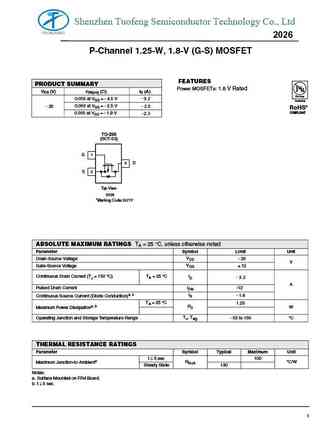
Shenzhen Tuofeng Semiconductor Technology Co., Ltd 2026 P-Channel 1.25-W, 1.8-V (G-S) MOSFET FEATURES PRODUCT SUMMARY Power MOSFETs 1.8 V Rated VDS (V) rDS(on) ( )ID (A) Pb-free - 0.056 at VGS = - 4.5 V 3.2 Available 0.069 at VGS = - 2.5 V - 20 - 2.8 RoHS* COMPLIANT 0.086 at VGS = - 1.8 V - 2.3 TO-236 (SOT-23) G 1 3 D S 2 Top View 2026 *Marking Code 262TF ABSOLUTE ... See More ⇒
0.1. Size:102K renesas
rej03g1161 hat2026rds.pdf
To our customers, Old Company Name in Catalogs and Other Documents On April 1st, 2010, NEC Electronics Corporation merged with Renesas Technology Corporation, and Renesas Electronics Corporation took over all the business of both companies. Therefore, although the old company name remains in this document, it is a valid Renesas Electronics document. We appreciate your understanding. ... See More ⇒
0.5. Size:234K cdil
cfa1046 cfc2026 y gr.pdf
Continental Device India Limited An ISO/TS 16949, ISO 9001 and ISO 14001 Certified Company PNP SILICON PLANAR POWER TRANSISTOR CFA1046 TO-220FP Fully Isolated Plastic Package Complementary CFC2026 ABSOLUTE MAXIMUM RATINGS DESCRIPTION SYMBOL VALUE UNIT Collector Base Voltage VCBO 60 V Collector Emitter Voltage VCEO 60 V Emitter Base Voltage VEBO 7.0 V RMS Isolation Voltage (for 1sec, ... See More ⇒
0.6. Size:128K cdil
cfc2026 cfa1046 y gr.pdf

Continental Device India Limited An ISO/TS 16949, ISO 9001 and ISO 14001 Certified Company NPN SILICON PLANAR POWER TRANSISTOR CFC2026 TO-220FP Fully Isolated Plastic Package Complementary CFA1046 ABSOLUTE MAXIMUM RATINGS DESCRIPTION SYMBOL VALUE UNIT Collector Base Voltage VCBO 60 V Collector Emitter Voltage VCEO 60 V Emitter Base Voltage VEBO 7.0 V RMS Isolation Voltage (for 1sec, ... See More ⇒
0.7. Size:40K kec
ktc2026.pdf
SEMICONDUCTOR KTC2026 TECHNICAL DATA EPITAXIAL PLANAR NPN TRANSISTOR GENERAL PURPOSE APPLICATION. A C FEATURES DIM MILLIMETERS S Low Collector Saturation Voltage _ A 10.0 0.3 + _ + B 15.0 0.3 VCE(sat)=1.0V(Max.) at IC=2A, IB=0.2A. E C _ 2.70 0.3 + D Complementary to KTA1046. 0.76+0.09/-0.05 _ E 3.2 0.2 + _ F 3.0 0.3 + _ 12.0 0.3 G + H 0.5+0.1/-0.05 _ 13.6... See More ⇒
0.8. Size:852K willsemi
wpm2026.pdf
WPM2026 WPM2026 Single P-Channel, -20V, -3.2A, Power MOSFET Http //www.sh-willsemi.com VDS (V) Rds(on) ( ) 0.056@ VGS= 4.5V -20 0.069@ VGS= 2.5V 0.086@ VGS= 1.8V SOT-23 Descriptions D The WPM2026 is P-Channel enhancement MOS 3 Field Effect Transistor. Uses advanced trench technology and design to provide excellent RDS (ON) with low gate charge. This device is suitab... See More ⇒
0.9. Size:317K cystek
mbnp2026g6.pdf
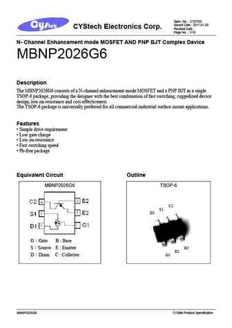
Spec. No. C197G6 Issued Date 2011.01.20 CYStech Electronics Corp. Revised Date Page No. 1/10 N- Channel Enhancement mode MOSFET AND PNP BJT Complex Device MBNP2026G6 Description The MBNP2026G6 consists of a N-channel enhancement-mode MOSFET and a PNP BJT in a single TSOP-6 package, providing the designer with the best combination of fast switching, ruggedized device ... See More ⇒
0.10. Size:110K tysemi
wpm2026.pdf
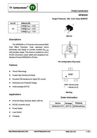
Product specification WPM2026 Single P-Channel, -20V, -3.2A, Power MOSFET VDS (V) Rds(on) ( ) 0.056@ VGS= 4.5V -20 0.069@ VGS= 2.5V 0.086@ VGS= 1.8V SOT-23 Descriptions D 3 The WPM2026 is P-Channel enhancement MOS Field Effect Transistor. Uses advanced trench technology and design to provide excellent RDS (ON) with low gate charge. This device is suitable for use in ... See More ⇒
0.11. Size:996K kexin
ktc2026.pdf
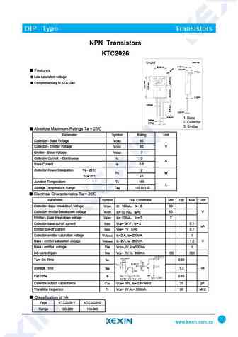
DIP Type Transistors NPN Transistors KTC2026 Unit mm TO-220F 0.20 0.20 0.20 2.54 Features 0.20 0.70 Low saturation voltage Complementary to KTA1046 0.20 2.76 1.47max 0.20 0.50 0.20 0.80 1. Base 2.54typ 2. Collector 2.54typ 3. Emitter Absolute Maximum Ratings Ta = 25 Parameter Symbol Rating Unit Collector - Base Voltage VCBO 60 C... See More ⇒
0.12. Size:681K slkor
sl2026.pdf
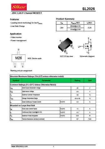
SL2026 -20V/-3.2A P-Channel MOSFET Product Summary Features Leading trench technology for low RDS(on) VDS RDS(ON) MAX ID MAX Low Gate Charge 65m @-4.5V D2 -20V S1 -3.2A D1 81m @-2.5V Application Video monitor Power management D S D G SOT-23 top view Schematic diagram M26 Device code M26 G S Marking and pin assignment Absolute Maximum Ratings (TA=25 u... See More ⇒
0.13. Size:1195K winsok
wst2026.pdf
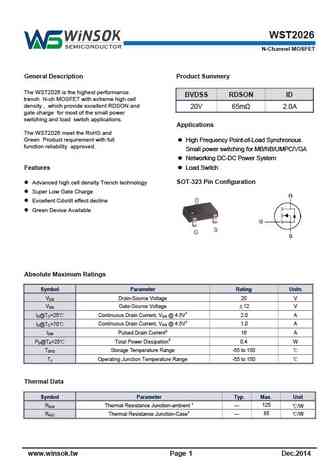
WST2026 N-Channel MOSFET General Description Product Summery The WST2026 is the highest performance BVDSS RDSON ID trench N-ch MOSFET with extreme high cell density , which provide excellent RDSON and 20V 65m 2.0A gate charge for most of the small power switching and load switch applications. Applications The WST2026 meet the RoHS and Green Product requirement with full ... See More ⇒
0.14. Size:175K inchange semiconductor
2sc2026.pdf
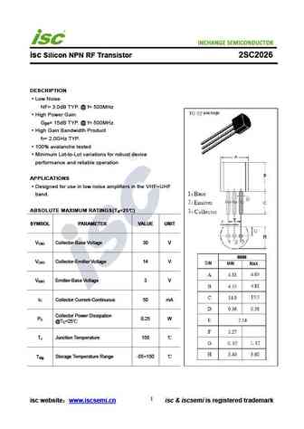
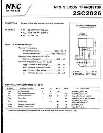
INCHANGE Semiconductor isc Silicon NPN RF Transistor 2SC2026 DESCRIPTION Low Noise NF= 3.0dB TYP. @ f= 500MHz High Power Gain G = 15dB TYP. @ f= 500MHz pe High Gain Bandwidth Product f = 2.0GHz TYP. T 100% avalanche tested Minimum Lot-to-Lot variations for robust device performance and reliable operation APPLICATIONS Designed for use in low noise amplifiers in the VHF... See More ⇒
0.15. Size:219K inchange semiconductor
2sk2026-01.pdf
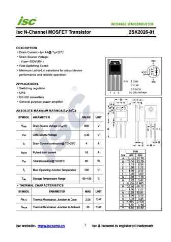
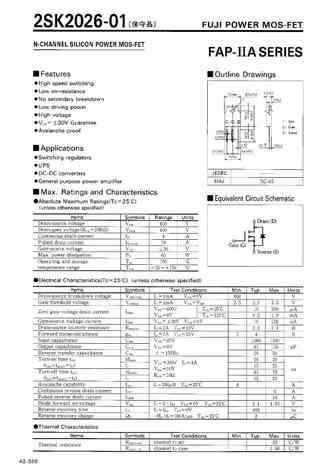
isc N-Channel MOSFET Transistor 2SK2026-01 DESCRIPTION Drain Current I = 4A@ T =25 D C Drain Source Voltage- V = 600V(Min) DSS Fast Switching Speed Minimum Lot-to-Lot variations for robust device performance and reliable operation APPLICATIONS Switching regulator UPS DC-DC converters General purpose power amplifier ABSOLUTE MAXIMUM RATINGS(T =25 ) a SY... See More ⇒
Detailed specifications: APM9986CO
, APM9988CO
, APM9988QA
, SIR164DP
, 1481
, 2015
, 2016
, 2021
, 8205A
, 2341
, 4401
, 4402
, 4407
, 4409
, 4410
, 4435
, 4501
.
Keywords - 2026 MOSFET specs
2026 cross reference
2026 equivalent finder
2026 pdf lookup
2026 substitution
2026 replacement
Learn how to find the right MOSFET substitute. A guide to cross-reference, check specs and replace MOSFETs in your circuits.