2341 Specs and Replacement
Type Designator: 2341
Type of Transistor: MOSFET
Type of Control Channel: P-Channel
Absolute Maximum Ratings
Pd ⓘ
- Maximum Power Dissipation: 0.75 W
|Vds|ⓘ - Maximum Drain-Source Voltage: 20 V
|Vgs|ⓘ - Maximum Gate-Source Voltage: 12 V
|Id| ⓘ - Maximum Drain Current: 2.8 A
Tj ⓘ - Maximum Junction Temperature: 150 °C
Electrical Characteristics
RDSonⓘ - Maximum Drain-Source On-State Resistance: 0.06 Ohm
Package: SOT23
- MOSFET ⓘ Cross-Reference Search
2341 datasheet
..1. Size:2296K shenzhen
2341.pdf 
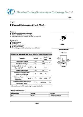
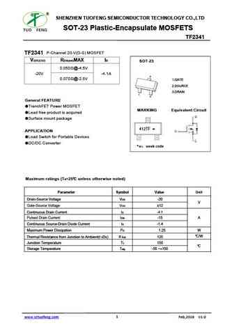
Shenzhen Tuofeng Semiconductor Technology Co., Ltd 2341 2341 P-Channel Enhancement Mode Mosfet Features Higher Efficiency Extending Battery Life Miniature SOT23 Surface Mount Package 3 Super high density cell design for extremely low RDS (ON) 1 2 Applications DC/DC Converter Load Switch SOT 23 Battery Powered System LCD Display inverter Power Manage... See More ⇒
0.1. Size:73K 1
2sk2341.pdf
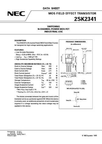
DATA SHEET MOS FIELD EFFECT TRANSISTOR 2SK2341 SWITCHING N-CHANNEL POWER MOS FET INDUSTRIAL USE DESCRIPTION PACKAGE DIMENSIONS The 2SK2341 is N-channel Power MOS Field Effect Transis- (in millimeters) tor designed for high voltage switching applications. 10.0 0.3 4.5 0.2 3.2 0.2 FEATURES 2.7 0.2 Low On-state Resistance RDS(on) = 0.26 MAX. (VGS = 10 V, ID = ... See More ⇒
0.2. Size:144K vishay
si2341.pdf
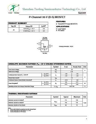
Shenzhen Tuofeng Semiconductor Technology Co., Ltd Si2341 P-Channel 30-V (D-S) MOSFET FEATURES PRODUCT SUMMARY D TrenchFETr Power MOSFETS VDS (V) rDS(on) (W) ID (A)b APPLICATIONS 0.072 @ VGS = -10 V -2.8 D Load Switch -30 30 D PA Switch 0.120 @ VGS = - 4.5 V -2.0 TO-236 (SOT-23) G 1 3 D Ordering Information Si2341 S 2 Top View ABSOLUTE MAXIMUM RATINGS (TA = 25_C UNLESS OTH... See More ⇒
0.3. Size:207K vishay
si2341ds.pdf
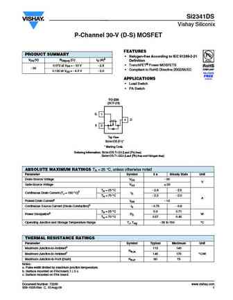
Si2341DS Vishay Siliconix P-Channel 30-V (D-S) MOSFET FEATURES PRODUCT SUMMARY Halogen-free According to IEC 61249-2-21 VDS (V) RDS(on) ( )ID (A)b Definition 0.072 at VGS = - 10 V - 2.8 TrenchFET Power MOSFETS - 30 Compliant to RoHS Directive 2002/95/EC 0.120 at VGS = - 4.5 V - 2.0 APPLICATIONS Load Switch PA Switch TO-236 (SOT-23) G 1 3 D S 2 T... See More ⇒
0.4. Size:2273K willsemi
wpm2341.pdf
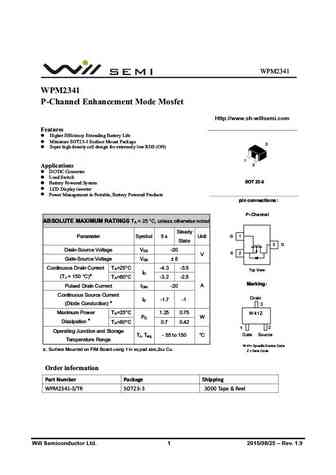
WPM2341 WPM2341 P-Channel Enhancement Mode Mosfet Http //www.sh-willsemi.com Features Higher Efficiency Extending Battery Life Miniature SOT23-3 Surface Mount Package 3 Super high density cell design for extremely low RDS (ON) 1 2 Applications DC/DC Converter Load Switch SOT 23-3 Battery Powered System LCD Display inverter Power Management in Porta... See More ⇒
0.5. Size:2125K willsemi
wpm2341a.pdf

WPM2341A WPM2341A P-Channel Enhancement Mode Mosfet Http //www.sh-willsemi.com Features Higher Efficiency Extending Battery Life Miniature SOT23-3 Surface Mount Package 3 Super high density cell design for extremely low RDS (ON) 1 2 Applications DC/DC Converter Load Switch SOT 23-3 Battery Powered System LCD Display inverter Power Management in Por... See More ⇒
0.6. Size:134K analog power
am2341p.pdf
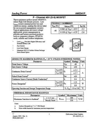
Analog Power AM2341P P - Channel 40V (D-S) MOSFET These miniature surface mount MOSFETs utilize High Cell Density process. Low PRODUCT SUMMARY rDS(on) assures minimal power loss and conserves energy, making this device ideal VDS (V) rDS(on) ( )ID (A) for use in power management circuitry. 0.082 @ VGS = -10 V -3.2 Typical applications are lower voltage -40 application, power ... See More ⇒
0.7. Size:490K alfa-mos
afp2341.pdf
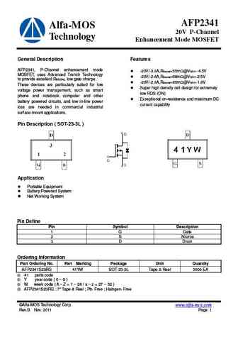
AFP2341 Alfa-MOS 20V P-Channel Technology Enhancement Mode MOSFET General Description Features AFP2341, P-Channel enhancement mode -20V/-3.0A,RDS(ON)=55m @VGS=- 4.5V MOSFET, uses Advanced Trench Technology -20V/-2.6A,RDS(ON)=68m @VGS=-2.5V to provide excellent RDS(ON), low gate charge. -20V/-2.0A,RDS(ON)=85m @VGS=-1.8V These devices are particularly suited for l... See More ⇒
0.8. Size:535K silikron
ssf2341e.pdf
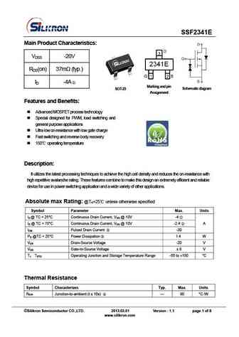
SSF2341E Main Product Characteristics VDSS -20V RDS(on) 37m (typ.) ID -4A Marking and pin SOT-23 Schematic diagram Assignme nt Features and Benefits Advanced MOSFET process technology Special designed for PWM, load switching and general purpose applications Ultra low on-resistance with low gate charge Fast switching and reverse body recovery ... See More ⇒
0.9. Size:596K tysemi
wpm2341a.pdf
Product specification WPM2341A P-Channel Enhancement Mode Mosfet Features Higher Efficiency Extending Battery Life Miniature SOT23-3 Surface Mount Package 3 Super high density cell design for extremely low RDS (ON) 1 2 Applications DC/DC Converter Load Switch SOT 23-3 Battery Powered System LCD Display inverter Power Management in Portable, Battery P... See More ⇒
0.10. Size:233K first silicon
ftk2341e.pdf
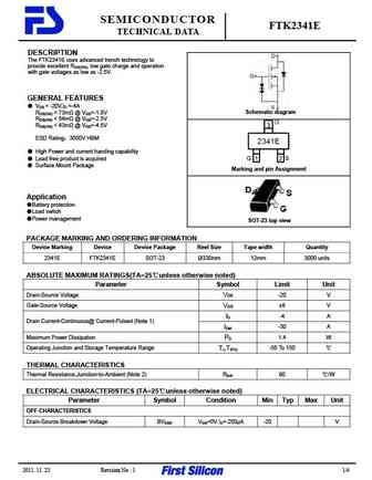
SEMICONDUCTOR FTK2341E TECHNICAL DATA DESCRIPTION The FTK2341E uses advanced trench technology to provide excellent RDS(ON), low gate charge and operation with gate voltages as low as -2.5V. GENERAL FEATURES VDS = -20V,ID =-4A Schematic diagram RDS(ON) ... See More ⇒
0.12. Size:1682K kexin
si2341ds.pdf
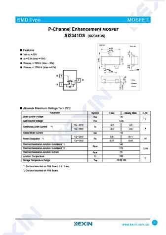
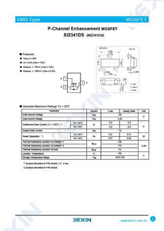
SMD Type MOSFET P-Channel Enhancement MOSFET SI2341DS (KI2341DS) SOT-23 Unit mm +0.1 2.9 -0.1 0.4+0.1 Features -0.1 3 VDS (V) =-30V ID =-2.8A (VGS =-10V) RDS(ON) 72m (VGS =-10V) 1 2 RDS(ON) 120m (VGS =-4.5V) +0.1 +0.05 0.95 -0.1 0.1-0.01 +0.1 1.9-0.1 G 1 1.Gate 3 D 2.Source S 2 3.Drain Absolute Maximum Ratings Ta = 25 Param... See More ⇒
0.13. Size:50K kexin
ki2341ds.pdf
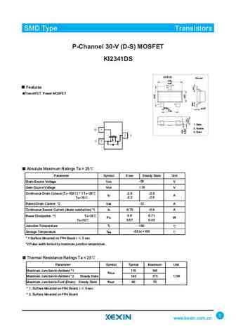
SMD Type IC SMD Type Transistors P-Channel 30-V (D-S) MOSFET KI2341DS SOT-23 Unit mm +0.1 2.9-0.1 +0.1 0.4-0.1 3 Features TrenchFET Power MOSFET 12 +0.1 +0.05 0.95-0.1 0.1-0.01 +0.1 1.9-0.1 1.Base 1. Gate 2.Emitter 2. Source 3. Drain 3.collector Absolute Maximum Ratings Ta = 25 Parameter Symbol 5 sec Steady State Unit Drain-Source Voltage VDS -30 V Gate-Source Volta... See More ⇒
0.14. Size:946K globaltech semi
gsm2341.pdf
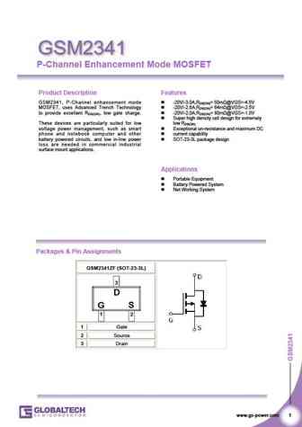
P-Channel Enhancement Mode MOSFET Product Description Features GSM2341, P-Channel enhancement mode -20V/-3.0A,RDS(ON)= 50m @VGS=-4.5V MOSFET, uses Advanced Trench Technology -20V/-2.6A,RDS(ON)= 64m @VGS=-2.5V to provide excellent RDS(ON), low gate charge. -20V/-2.0A,RDS(ON)= 80m @VGS=-1.8V Super high density cell design for extremely These devices are particularly suited... See More ⇒
0.15. Size:674K slkor
wpm2341.pdf
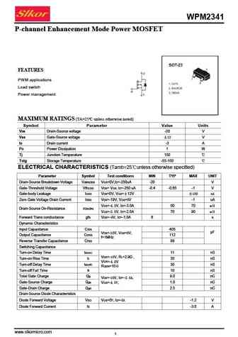
WPM2341 P-channel Enhancement Mode Power MOSFET FEATURES PWM applications Load switch Power management MAXIMUM RATINGS (TA=25 unless otherwise noted) Symbol Parameter Value Units VDS Drain-Source voltage -20 V VGS Gate-Source voltage 12 V ID Drain current -3 A PD Power Dissipation 1 W Tj Junction Temperature 150 Tstg Storage Temperature -55-150 ELECTRICAL CHARACTERIST... See More ⇒
0.16. Size:598K stansontech
st2341srg.pdf
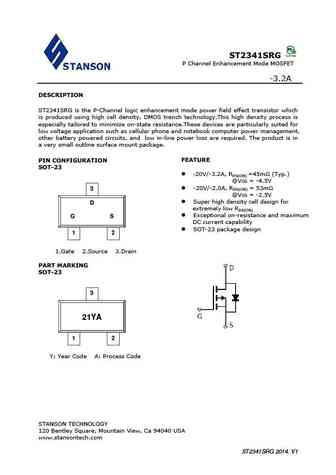
ST2341SRG P Channel Enhancement Mode MOSFET -3.2A DESCRIPTION ST2341SRG is the P-Channel logic enhancement mode power field effect transistor which is produced using high cell density, DMOS trench technology.This high density process is especially tailored to minimize on-state resistance.These devices are particularly suited for low voltage application such as cellular phone and... See More ⇒
0.17. Size:576K stansontech
st2341a.pdf
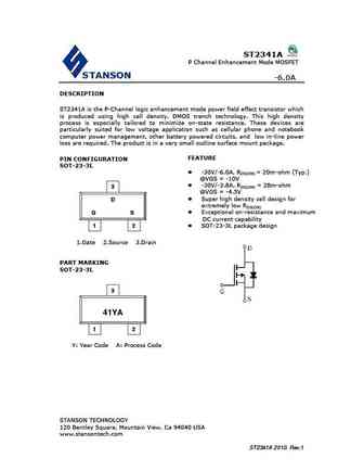
ST2341A P Channel Enhancement Mode MOSFET -6.0A DESCRIPTION ST2341A is the P-Channel logic enhancement mode power field effect transistor which is produced using high cell density, DMOS trench technology. This high density process is especially tailored to minimize on-state resistance. These devices are particularly suited for low voltage application such as cellular phone and n... See More ⇒
0.18. Size:602K stansontech
st2341s23rg.pdf
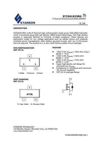
ST2341S23RG P Channel Enhancement Mode MOSFET -5.3A DESCRIPTION ST2341S23RG is the P-Channel logic enhancement mode power field effect transistor which is produced using high cell density, DMOS trench technology. This high density process is especially tailored to minimize on-state resistance. These devices are particularly suited for low voltage application such as cellular pho... See More ⇒
0.19. Size:1742K anbon
as2341.pdf
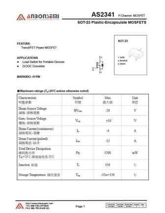
AS2341 P-Channel MOSFET SOT-23 Plastic-Encapsulate MOSFETS SOT-23 FEATURE TrenchFET Power MOSFET 1. GATE APPLICATIONS 2. SOURCE Load Switch for Portable Devices 3. DRAIN DC/DC Converter MARKING 41 YW Maximum ratings (Ta=25 unless otherwise noted) Characteristic Symbol Max Unit Drain-Source Voltage BV -20 V DSS ... See More ⇒
0.20. Size:273K msksemi
wpm2341-ms.pdf
www.msksemi.com WPM2341-MS Semiconductor Compiance APPLICATION Load Switch for Portable Devices DC/DC Converter FEATURE TrenchFET Power MOSFET I V(BR)DSS RDS(on)MAX D 90 m @-4.5V -20 V -3 A 110 m @-2.5V 1. GATE 2. SOURCE 3. DRAIN SOT-23-3L Maximum ratings (Ta=25 unless otherwise noted) Parameter Symbol Value Unit Drain-Source Voltage V -20 DS V Gate-Sour... See More ⇒
0.22. Size:868K cn vbsemi
wpm2341a-3-tr.pdf
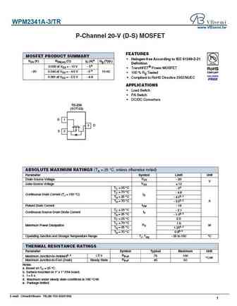
WPM2341A-3/TR www.VBsemi.tw P-Channel 20-V (D-S) MOSFET FEATURES MOSFET PRODUCT SUMMARY Halogen-free According to IEC 61249-2-21 VDS (V) RDS(on) ( )ID (A)a Qg (Typ.) Definition 0.035 at VGS = - 10 V - 5e TrenchFET Power MOSFET e - 20 0.043 at VGS = - 4.5 V - 5 10 nC 100 % Rg Tested 0.061 at VGS = - 2.5 V - 4.8 Compliant to RoHS Directive 2002/95/EC APPLIC... See More ⇒
0.23. Size:911K cn vbsemi
ssf2341e.pdf
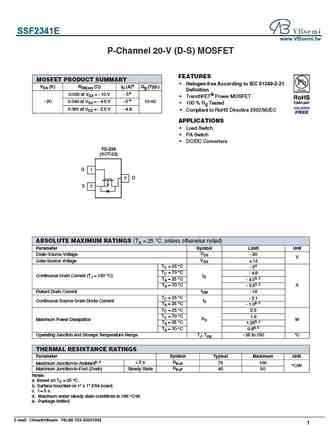
SSF2341E www.VBsemi.tw P-Channel 20-V (D-S) MOSFET FEATURES MOSFET PRODUCT SUMMARY Halogen-free According to IEC 61249-2-21 VDS (V) RDS(on) ( )ID (A)a Qg (Typ.) Definition 0.035 at VGS = - 10 V - 5e TrenchFET Power MOSFET e - 20 0.043 at VGS = - 4.5 V - 5 10 nC 100 % Rg Tested 0.061 at VGS = - 2.5 V - 4.8 Compliant to RoHS Directive 2002/95/EC APPLICATION... See More ⇒
0.24. Size:906K cn vbsemi
st2341s23r.pdf
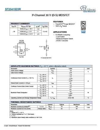
ST2341S23R www.VBsemi.tw P-Channel 30 V (D-S) MOSFET FEATURES PRODUCT SUMMARY TrenchFET Power MOSFET 100 % Rg Tested VDS (V) RDS(on) ( ) Typ. ID (A)a Qg (Typ.) 0.046 at VGS = - 10 V - 5.6 0.049 at VGS = - 6 V - 5 11.4 nC - 30 APPLICATIONS 0.054 at VGS = - 4.5 V -4.5 For Mobile Computing - Load Switch - Notebook Adaptor Switch S TO-236 - DC/DC Converter (SOT-... See More ⇒
0.25. Size:610K cn hmsemi
hm2341.pdf

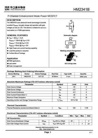
HM2341 P-Channel Enhancement Mode Power MOSFET DESCRIPTION D The HM2341 uses advanced trench technology to provide excellent RDS(ON), low gate charge and operation with gate G voltages as low as 2.5V. This device is suitable for use as a load switch or in PWM applications. S Schematic diagram GENERAL FEATURES VDS = -30V,ID = -4.2A RDS(ON) ... See More ⇒
0.26. Size:553K cn hmsemi
hm2341b.pdf
HM2341B P-Channel Enhancement Mode Power MOSFET DESCRIPTION D The HM2341B uses advanced trench technology to provide excellent RDS(ON), low gate charge and operation with gate G voltages as low as 2.5V. This device is suitable for use as a load switch or in PWM applications. S Schematic diagram GENERAL FEATURES VDS = -30V,ID = -4.2A RDS(ON) ... See More ⇒
Detailed specifications: APM9988CO
, APM9988QA
, SIR164DP
, 1481
, 2015
, 2016
, 2021
, 2026
, 7N65
, 4401
, 4402
, 4407
, 4409
, 4410
, 4435
, 4501
, 4542
.
Keywords - 2341 MOSFET specs
2341 cross reference
2341 equivalent finder
2341 pdf lookup
2341 substitution
2341 replacement
Need a MOSFET replacement?
Our guide shows you how to find a perfect substitute by comparing key parameters and specs