4402 Specs and Replacement
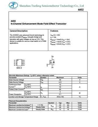
Type Designator: 4402
Type of Transistor: MOSFET
Type of Control Channel: N-Channel
Absolute Maximum Ratings
Pd ⓘ
- Maximum Power Dissipation: 3 W
|Vds|ⓘ - Maximum Drain-Source Voltage: 30 V
|Vgs|ⓘ - Maximum Gate-Source Voltage: 12 V
|Id| ⓘ - Maximum Drain Current: 12 A
Tj ⓘ - Maximum Junction Temperature: 150 °C
Electrical Characteristics
RDSonⓘ - Maximum Drain-Source On-State Resistance: 0.014 Ohm
Package: SOP8
- MOSFET ⓘ Cross-Reference Search
4402 datasheet
..1. Size:975K shenzhen
4402.pdf 

Shenzhen Tuofeng Semiconductor Technology Co., Ltd 4402 4402 N-Channel Enhancement Mode Field Effect Transistor General Description Features The AO4402 uses advanced trench technology to VDS (V) = 30V provide excellent RDS(ON), low gate charge and ID = 12A operation with gate voltages as low as 2.5V. This RDS(ON) ... See More ⇒
0.2. Size:297K motorola
2n4402 2n4403.pdf 

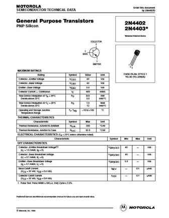
MOTOROLA Order this document SEMICONDUCTOR TECHNICAL DATA by 2N4402/D General Purpose Transistors 2N4402 PNP Silicon * 2N4403 *Motorola Preferred Device COLLECTOR 3 2 BASE 1 EMITTER 1 2 3 MAXIMUM RATINGS CASE 29 04, STYLE 1 Rating Symbol Value Unit TO 92 (TO 226AA) Collector Emitter Voltage VCEO 40 Vdc Collector Base Voltage VCBO 40 Vdc Emitter Base Voltage ... See More ⇒
0.3. Size:28K sanyo
ec4402c.pdf 

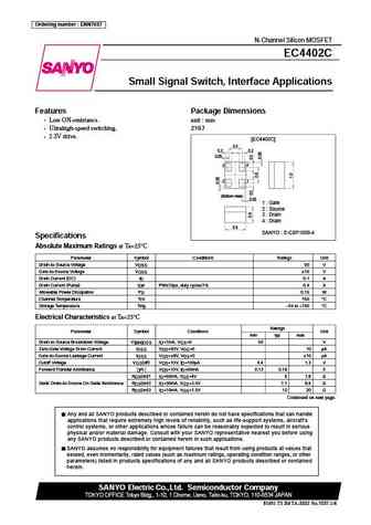
Ordering number ENN7037 EC4402C N-Channel Silicon MOSFET EC4402C Small Signal Switch, Interface Applications Features Package Dimensions Low ON-resistance. unit mm Ultrahigh-speed switching. 2197 2.5V drive. [EC4402C] 0.5 0.2 0.2 0.05 3 4 2 1 (Bottom view) 0.05 1 Gate 2 Source 3 Drain 4 Drain 0.8 SANYO E-CSP1008-4 Specifications Absolute Maximum... See More ⇒
0.4. Size:120K sanyo
2sc4402.pdf 

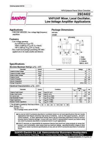
Ordering number EN2755 NPN Epitaxial Planar Silicon Transistor 2SC4402 VHF/UHF Mixer, Local Oscillator, Low-Voltage Amplifier Applications Applications Package Dimensions VHF/UHF MIX/OSC, low-voltage high-frequency unit mm amplifiers. 2059B [2SC4402] 0.3 Features 0.15 Low-voltage operation 3 fT=3.0GHz typ (VCE=3V) 0 0.1 MAG=12dB typ (VCE=3V, IC=10mA) NF=1.5dB ty... See More ⇒
0.5. Size:67K fairchild semi
2n4402.pdf 

2N4402 C TO-92 B E PNP General Purpose Amplifier This device is designed for use as general purpose amplifiers and switches requiring collector currents to 500 mA. Absolute Maximum Ratings* TA = 25 C unless otherwise noted Symbol Parameter Value Units VCEO Collector-Emitter Voltage 40 V V Collector-Base Voltage 40 V CBO VEBO Emitter-Base Voltage5.0V ICCollector Current - Continuo... See More ⇒
0.6. Size:258K nxp
pmcm4402upe.pdf 

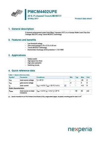
PMCM4402UPE 20 V, P-channel Trench MOSFET 30 May 2017 Product data sheet 1. General description P-channel enhancement mode Field-Effect Transistor (FET) in a 4 bumps Wafer Level Chip-Size Package (WLCSP) using Trench MOSFET technology. 2. Features and benefits Low threshold voltage Ultra small package 0.78 x 0.78 x 0.35 mm Trench MOSFET technology ElectroStatic Dischar... See More ⇒
0.7. Size:54K samsung
2n4402-2n4403.pdf 

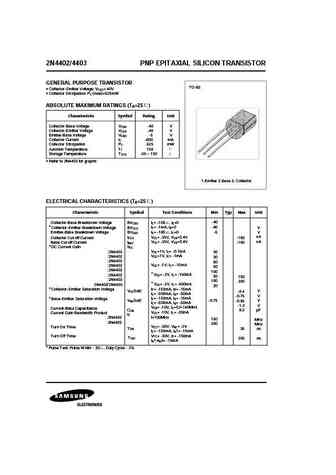
2N4402/4403 PNP EPITAXIAL SILICON TRANSISTOR GENERAL PURPOSE TRANSISTOR TO-92 Collector-Emitter Voltage VCEO= 40V Collector Dissipation PC (max)=625mW ABSOLUTE MAXIMUM RATINGS (T =25 ) A Characteristic Symbol Rating Unit Collector-Base Voltage VCBO -40 V Collector-Emitter Voltage VCEO -40 V Emitter-Base Voltage VEBO -5 V Collector Current IC -600 mA Collector Dissipation ... See More ⇒
0.9. Size:30K diodes
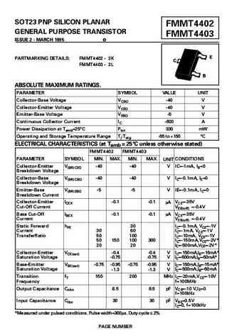
fmmt4402 fmmt4403.pdf 

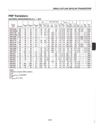
SOT23 PNP SILICON PLANAR 402 FMMT4402 GENERAL PURPOSE TRANSISTOR 403 FMMT4403 ISSUE 2 - MARCH 1995 E T I D T I T C T V B ABSOLUTE MAXIMUM RATINGS. T V IT II V I V V II i V I V V i V I V V i II I Di i i T i T T T ELECTRICAL CHARACTERISTICS (at Tamb = 25 C unless otherwise stated) T T T I I IT DITI II i V V I I V I II V V I I V I i V ... See More ⇒
0.11. Size:104K secos
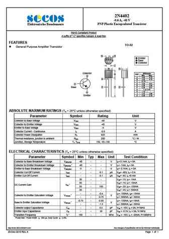
2n4402.pdf 

2N4402 -0.6 A, -40 V PNP Plastic Encapsulated Transistor Elektronische Bauelemente RoHS Compliant Product A suffix of -C specifies halogen & lead-free FEATURES TO-92 General Purpose Amplifier Transistor G H Emitter Base Collector J A D Collector Millimeter B REF. Min. Max. A 4.40 4.70 K B 4.30 4.70 C 12.70 - D 3.30 3.81 E ... See More ⇒
0.12. Size:596K secos
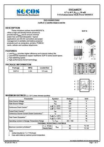
ssg4402n.pdf 

SSG4402N 6.7 A, 60 V, RDS(ON) 38 m N-Ch Enhancement Mode Power MOSFET Elektronische Bauelemente RoHS Compliant Product A suffix of -C specifies halogen & lead-free DESCRIPTION These miniature surface mount MOSFETs SOP-8 utilize a high cell density trench process to provide low RDS(on) and to ensure minimal power loss and heat dissipation. Typical applications ar... See More ⇒
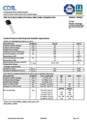
0.13. Size:355K cdil
2n4402 3.pdf 

Continental Device India Limited An ISO/TS 16949, ISO 9001 and ISO 14001 Certified Company 2N4402 / 2N4403 PNP SILICON PLANAR EPITAXIAL SWITCHING TRANSISTORS TO-92 Plastic Package For Lead Free Parts, Device Part # will be Prefixed with "T" C B E General Purpose Switching And Amplifier Applications ABSOLUTE MAXIMUM RATINGS (Ta=25 C) DESCRIPTION SYMBOL VALUE UNITS Collector Emi... See More ⇒
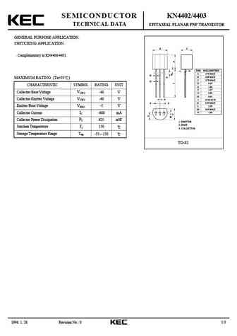
0.14. Size:430K kec
kn4402 kn4403.pdf 

SEMICONDUCTOR KN4402/4403 TECHNICAL DATA EPITAXIAL PLANAR PNP TRANSISTOR GENERAL PURPOSE APPLICATION. SWITCHING APPLICATION. B C Complementary to KN4400/4401. N DIM MILLIMETERS A 4.70 MAX E K B 4.80 MAX G MAXIMUM RATING (Ta=25 ) C 3.70 MAX D D 0.45 CHARACTERISTIC SYMBOL RATING UNIT E 1.00 F 1.27 VCBO -40 V Collector-Base Voltage G 0.85 H 0.45 _ VCEO -40 V Collector-... See More ⇒
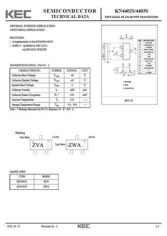
0.15. Size:38K kec
kn4402s kn4403s.pdf 

SEMICONDUCTOR KN4402S/4403S TECHNICAL DATA EPITAXIAL PLANAR PNP TRANSISTOR GENERAL PURPOSE APPLICATION. SWITCHING APPLICATION. E L B L FEATURES DIM MILLIMETERS Complementary to the KN4400S/4401S _ + A 2.93 0.20 B 1.30+0.20/-0.15 Suffix U Qualified to AEC-Q101. C 1.30 MAX 2 3 D 0.40+0.15/-0.05 ex) KN4403S-RTK/HU E 2.40+0.30/-0.20 1 G 1.90 H 0.95 J 0.13+0.10/-0.05 K... See More ⇒
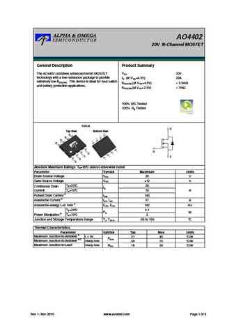
0.16. Size:275K aosemi
ao4402.pdf 

AO4402 20V N-Channel MOSFET General Description Product Summary VDS 20V The AO4402 combines advanced trench MOSFET technology with a low resistance package to provide ID (at VGS=4.5V) 20A extremely low RDS(ON). This device is ideal for load switch RDS(ON) (at VGS=4.5V) ... See More ⇒
0.17. Size:343K aosemi
ao4402g.pdf 

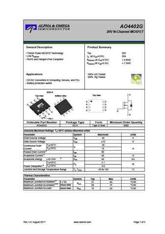
AO4402G 20V N-Channel MOSFET General Description Product Summary VDS Trench Power MOSFET technology 20V Low RDS(ON) ID (at VGS=4.5V) 20A RoHS and Halogen-Free Compliant RDS(ON) (at VGS=4.5V) ... See More ⇒
0.18. Size:320K analog power
am4402n.pdf 

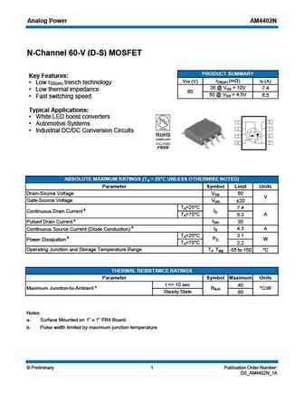
Analog Power AM4402N N-Channel 60-V (D-S) MOSFET PRODUCT SUMMARY Key Features rDS(on) (m ) VDS (V) ID (A) Low r trench technology DS(on) 38 @ VGS = 10V 7.4 Low thermal impedance 60 50 @ VGS = 4.5V 6.5 Fast switching speed Typical Applications White LED boost converters Automotive Systems Industrial DC/DC Conversion Circuits ABSOLUTE MAXIMUM ... See More ⇒
0.19. Size:308K cystek
mtn4402q8.pdf 

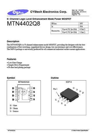
Spec. No. C910Q8 Issued Date 2013.05.21 CYStech Electronics Corp. Revised Date Page No. 1/9 N -Channel Logic Level Enhancement Mode Power MOSFET BVDSS 20V MTN4402Q8 ID 20A 4.3m VGS=4.5V, ID=20A RDSON(TYP) 5.3m VGS=2.5V, ID=20A Description The MTN4402Q8 is a N-channel enhancement-mode MOSFET, providing the designer with the best combination of fast switc... See More ⇒
0.20. Size:386K unikc
p4402fag.pdf 

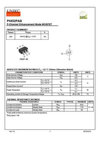
P4402FAG P-Channel Enhancement Mode MOSFET PRODUCT SUMMARY V(BR)DSS RDS(ON) ID -20V 44m @VGS = -4.5V -5A TSOP- 06 ABSOLUTE MAXIMUM RATINGS (TA = 25 C Unless Otherwise Noted) PARAMETERS/TEST CONDITIONS SYMBOL LIMITS UNITS VDS Drain-Source Voltage -20 V VGS Gate-Source Voltage 12 TA = 25 C -4.2 ID Continuous Drain Current TA = 70 A C -3.3 IDM -20 Pulsed Drain ... See More ⇒
0.21. Size:330K semtech
2n4402 2n4403.pdf 

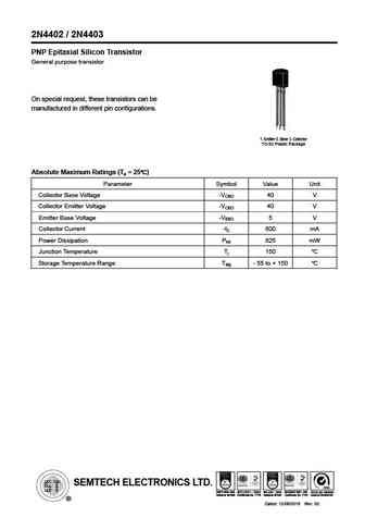
2N4402 / 2N4403 PNP Epitaxial Silicon Transistor General purpose transistor On special request, these transistors can be manufactured in different pin configurations. 1. Emitter 2. Base 3. Collector TO-92 Plastic Package Absolute Maximum Ratings (Ta = 25 ) Parameter Symbol Value Unit Collector Base Voltage -VCBO 40 V Collector Emitter Voltage -VCEO 40 V Emitter Base Voltage... See More ⇒
0.22. Size:1484K kexin
ao4402.pdf 

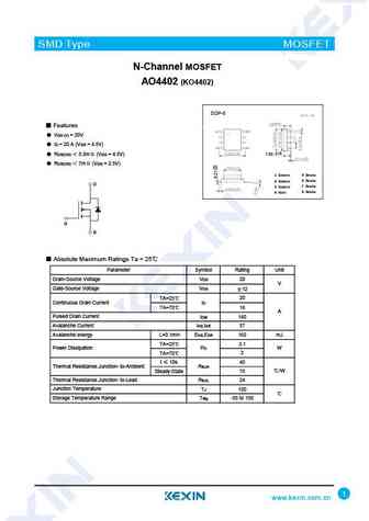
SMD Type MOSFET N-Channel MOSFET AO4402 (KO4402) SOP-8 Features VDS (V) = 20V ID = 20 A (VGS = 4.5V) 1.50 0.15 RDS(ON) 5.5m (VGS = 4.5V) RDS(ON) 7m (VGS = 2.5V) 1 Source 5 Drain 6 Drain 2 Source D 7 Drain 3 Source 8 Drain 4 Gate G S Absolute Maximum Ratings Ta = 25 Parameter Symbol Rating Unit Drain-Source Voltage VDS 20 V Gat... See More ⇒
0.23. Size:654K elm
elm34402aa.pdf 

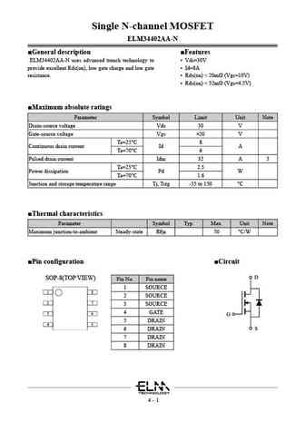
Single N-channel MOSFET ELM34402AA-N General description Features ELM34402AA-N uses advanced trench technology to Vds=30V provide excellent Rds(on), low gate charge and low gate Id=8A resistance. Rds(on) ... See More ⇒
0.24. Size:43K sensitron
shd724402.pdf 

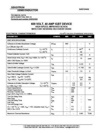
SENSITRON SHD724402 SEMICONDUCTOR TECHNICAL DATA DATA SHEET 994, REV. B Formerly part number SHDG1024 600 VOLT, 40 AMP IGBT DEVICE HIGH SPEED, IMPROVED SCSOA WITH FAST REVERSE RECOVERY DIODE ELECTRICAL CHARACTERISTICS (Tj=250C UNLESS OTHERWISE SPECIFIED) PARAMETER SYMBOL MIN TYP MAX UNIT PARAMETER SYMBOL MIN TYP MAX UNIT IGBT SPECIFICATIONS Collector to Emitter Breakdown... See More ⇒
0.25. Size:356K stansontech
stn4402.pdf 

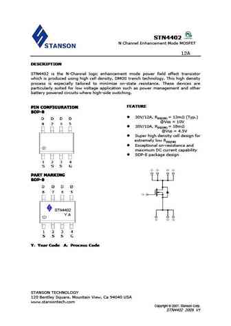
STN4402 STN4402 STN4402 STN4402 N Channel Enhancement Mode MOSFET 12A DESCRIPTION DESCRIPTION DESCRIPTION DESCRIPTION STN4402 is the N-Channel logic enhancement mode power field effect transistor which is produced using high cell density, DMOS trench technology. This high density process is especially tailored to minimize on-state resistance. These devices are particularly suited f... See More ⇒
0.28. Size:464K cn hmsemi
hm4402c.pdf 

HM4402C N-Channel Enhancement Mode Power MOSFET Description The HM4402C uses advanced trench technology and design to provide excellent RDS(ON) with low gate charge. It can be used in a wide variety of applications. General Features VDS =20V,ID =12A Schematic diagram RDS(ON) ... See More ⇒
0.29. Size:489K cn hmsemi
hm4402e.pdf 

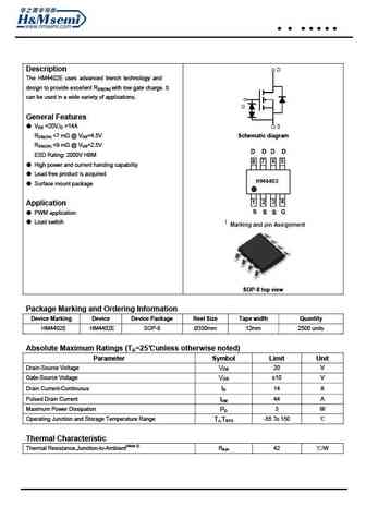
HM4402E Description The HM4402E uses advanced trench technology and design to provide excellent RDS(ON) with low gate charge. It can be used in a wide variety of applications. General Features VDS =20V,ID =14A RDS(ON) ... See More ⇒
0.30. Size:621K cn hmsemi
hm4402b.pdf 

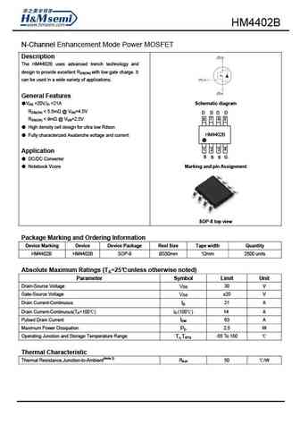
HM4402B N-Channel Enhancement Mode Power MOSFET Description The HM4402B uses advanced trench technology and design to provide excellent RDS(ON) with low gate charge. It can be used in a wide variety of applications. General Features VDS =20V,ID =21A Schematic diagram RDS(ON) ... See More ⇒
0.31. Size:626K cn hmsemi
hm4402a.pdf 

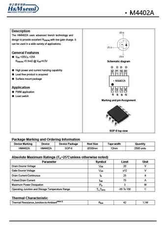
H Description The uses advanced trench technology and design to provide excellent RDS(ON) with low gate charge. It can be used in a wide variety of applications. General Features VDS =20V,ID = A RDS(ON) ... See More ⇒
Detailed specifications: SIR164DP
, 1481
, 2015
, 2016
, 2021
, 2026
, 2341
, 4401
, IRF630
, 4407
, 4409
, 4410
, 4435
, 4501
, 4542
, 4606
, 4611
.
Keywords - 4402 MOSFET specs
4402 cross reference
4402 equivalent finder
4402 pdf lookup
4402 substitution
4402 replacement
Step-by-step guide to finding a MOSFET replacement. Cross-reference parts and ensure compatibility for your repair or project.
