4953 Specs and Replacement
Type Designator: 4953
Type of Transistor: MOSFET
Type of Control Channel: P-Channel
Absolute Maximum Ratings
Pd ⓘ - Maximum Power Dissipation: 2 W
|Vds|ⓘ - Maximum Drain-Source Voltage: 30 V
|Vgs|ⓘ - Maximum Gate-Source Voltage: 20 V
|Id| ⓘ - Maximum Drain Current: 5.3 A
Tj ⓘ - Maximum Junction Temperature: 175 °C
Electrical Characteristics
RDSonⓘ - Maximum Drain-Source On-State Resistance: 0.06 Ohm
Package: SOP8
4953 substitution
- MOSFET ⓘ Cross-Reference Search
4953 datasheet
4953.pdf
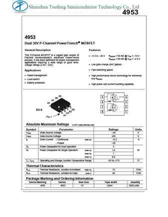
Shenzhen Tuofeng Semiconductor Technology Co., Ltd 4953 4953 Dual 30V P-Channel PowerTrench MOSFET General Description Features This P MOSFET is a rugged gate version of -Channel 5.3 A, 30 V R = 59 m @ V = 10 V DS(ON) GS Fairchild Semiconductor s advanced PowerTrench R = 89 m @ V = 4.5 V DS(ON) GS process. It has been optimized for power management ... See More ⇒
4953.pdf
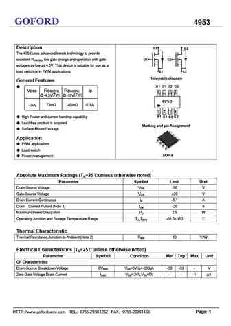
GOFORD 4953 Description D1 D2 The 4953 uses advanced trench technology to provide excellent RDS(ON), low gate charge and operation with gate G1 G2 voltages as low as 4.5V. This device is suitable for use as a load switch or in PWM applications. S1 S2 Schematic diagram General Features VDSS RDS(ON) RDS(ON) ID @ (Typ) @ -4.5V -10V (Typ) m m -30V 73 48 -5.1 A ... See More ⇒
4953.pdf
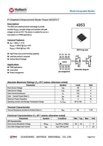
Plastic-Encapsulate Mosfets P-Channel Enhancement Mode Power MOSFET Description 4953 The 4953 uses advanced trench technology to provide excellent RDS(ON), low gate charge and operation with gate voltages as low as 4.5V. This device is suitable for use as a load switch or in PWM applications. General Features VDS = -30V,ID = -5.1A RDS(ON) ... See More ⇒
4953.pdf
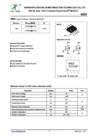
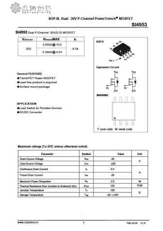
SHENZHEN TUOFENG SEMICONDUCTOR TECHNOLOGY CO.,LTD SOP-8L Dual -30V P-Channel PowerTrench MOSFET 4953 Dual 4953 P-Channel -30V(D-S) MOSFET V(BR)DSS RDS(on)MAX ID SOP-8 D2 D2 0.059 @-10V . D1 -30V -5.3A D1 0.089 @-4.5V G2 G S2 G1 S S S1 SO-8 S Pin 1 Equivalent Cir cuit D1 D2 General FEATURE TrenchFET Power MOSFET Lead free product is acquired Surface mount p... See More ⇒
me4953.pdf
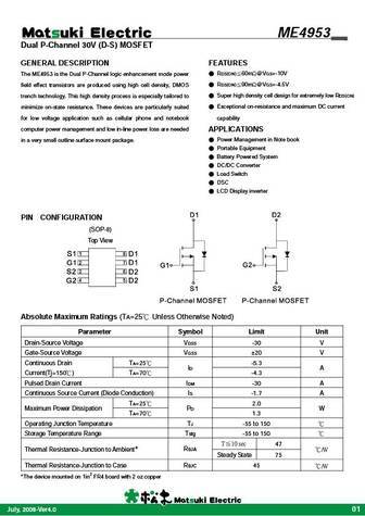
ME4953 Dual P-Channel 30V (D-S) MOSFET GENERAL DESCRIPTION FEATURES The ME4953 is the Dual P-Channel logic enhancement mode power RDS(ON) 60m @VGS=-10V field effect transistors are produced using high cell density, DMOS RDS(ON) 90m @VGS=-4.5V trench technology. This high density process is especially tailored to Super high density cell design for extremely low RDS(... See More ⇒
2n4953.pdf
2N4953 NPN General Purpose Amplifier This device designed for use as general purpose amplifier and switches requiring collector currents to 500mA. Sourced from Process 10. TO-92 1 1. Emitter 2. Collector 3. Base NPN Epitaxial Silicon Transistor Absolute Maximum Ratings* Ta=25 C unless otherwise noted Symbol Parameter Value Units VCEO Collector-Emitter Voltage 30 V VCBO C... See More ⇒
fds4953.pdf
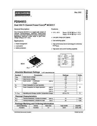
May 2002 FDS4953 Dual 30V P-Channel PowerTrench MOSFET General Description Features This P MOSFET is a rugged gate version of -Channel 5 A, 30 V R = 55 m @ V = 10 V DS(ON) GS Fairchild Semiconductor s advanced PowerTrench R = 95 m @ V = 4.5 V DS(ON) GS process. It has been optimized for power management applications requiring a wide range of gave d... See More ⇒
sq4953ey.pdf
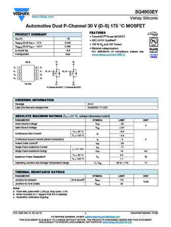
SQ4953EY www.vishay.com Vishay Siliconix Automotive Dual P-Channel 30 V (D-S) 175 C MOSFET FEATURES PRODUCT SUMMARY TrenchFET Power MOSFET VDS (V) - 30 AEC-Q101 Qualifiedc RDS(on) ( ) at VGS = - 10 V 0.045 100 % Rg and UIS Tested RDS(on) ( ) at VGS = - 4.5 V 0.085 Material categorization ID (A) per leg - 6.6 For definitions of compliance please see Co... See More ⇒
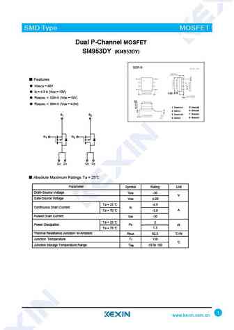
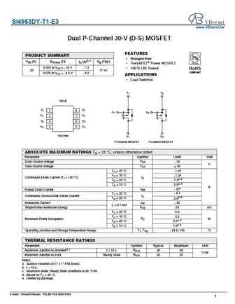
si4953ady.pdf
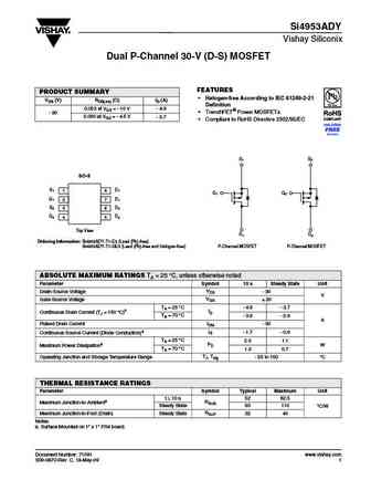
Si4953ADY Vishay Siliconix Dual P-Channel 30-V (D-S) MOSFET FEATURES PRODUCT SUMMARY Halogen-free According to IEC 61249-2-21 VDS (V) RDS(on) ( )ID (A) Definition 0.053 at VGS = - 10 V - 4.9 TrenchFET Power MOSFETs - 30 0.090 at VGS = - 4.5 V - 3.7 Compliant to RoHS Directive 2002/95/EC S1 S2 SO-8 S1 1 D1 8 G1 G2 G1 2 D1 7 S2 3 D2 6 G2 4 D2 5 To... See More ⇒
si4953dy.pdf
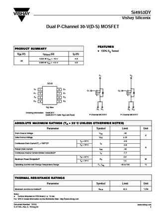
Si4953DY Vishay Siliconix Dual P-Channel 30-V(D-S) MOSFET FEATURES PRODUCT SUMMARY D 100% Rg Tested VDS (V) rDS(on) (W) ID (A) 0.053 @ VGS = -10 V -4.9 -30 30 0.095 @ VGS = -4.5 V -3.6 S1 S2 SO-8 S1 1 D1 8 G1 G2 G1 2 D1 7 S2 3 D2 6 G2 4 D2 5 Top View D1 D1 D2 D2 Ordering Information Si4953DY Si4953DY-T1 (with Tape and Reel) P-Channel MOSFET P-Channel MOSFET ABSOLUTE M... See More ⇒
mcq4953.pdf
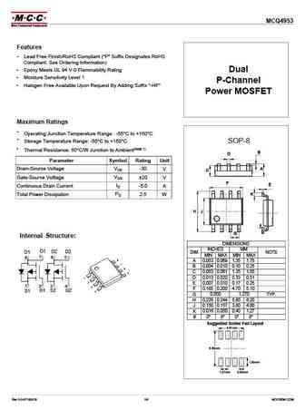
MCQ4953 Features Lead Free Finish/RoHS Compliant ("P" Suffix Designates RoHS Compliant. See Ordering Information) Epoxy Meets UL 94 V-0 Flammability Rating Dual Moisture Sensitivity Level 1 P-Channel Halogen Free Available Upon Request By Adding Suffix "-HF" Power MOSFET Maximum Ratings Operating Junction Temperature Range -55 C to +150 C Storage Temp... See More ⇒
2sc4953.pdf
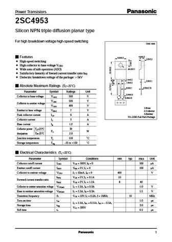
Power Transistors 2SC4953 Silicon NPN triple diffusion planar type For high breakdown voltage high-speed switching Unit mm 4.6 0.2 Features 9.9 0.3 2.9 0.2 High-speed switching High collector to base voltage VCBO 3.2 0.1 Wide area of safe operation (ASO) Satisfactory linearity of foward current transfer ratio hFE Dielectric breakdown voltage of the package > 5kV 1.4... See More ⇒
utm4953l-s08-r utm4953g-s08-r.pdf
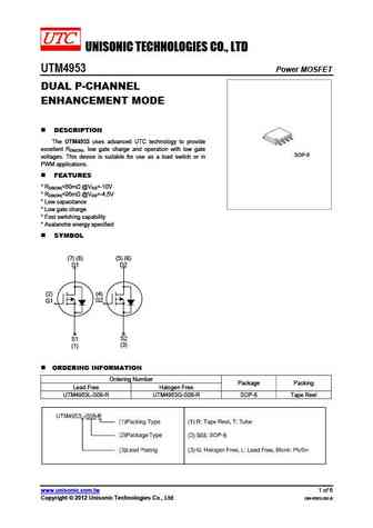
UNISONIC TECHNOLOGIES CO., LTD UTM4953 Power MOSFET DUAL P-CHANNEL ENHANCEMENT MODE DESCRIPTION The UTM4953 uses advanced UTC technology to provide excellent RDS(ON), low gate charge and operation with low gate SOP-8 voltages. This device is suitable for use as a load switch or in PWM applications. FEATURES * RDS(ON)... See More ⇒
utm4953.pdf
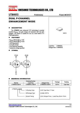
UNISONIC TECHNOLOGIES CO., LTD UTM4953 Preliminary Power MOSFET DUAL P-CHANNEL ENHANCEMENT MODE DESCRIPTION The UTM4953 uses advanced UTC technology to provide excellent RDS(ON), low gate charge and operation with low gate SOP-8 voltages. This device is suitable for use as a load switch or in PWM applications. FEATURES * RDS(ON)... See More ⇒
ssg4953p.pdf
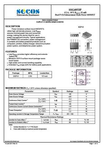
SSG4953P -5.2 A, -30 V, RDS(ON) 52 m Dual P-Ch Enhancement Mode Power MOSFET Elektronische Bauelemente RoHS Compliant Product A suffix of -C specifies halogen & lead-free DESCRIPTION SOP-8 These miniature surface mount MOSFETs utilize high cell density process. Low RDS(on) B assures minimal power loss and conserves energy, making this device ideal for use in po... See More ⇒
ssg4953.pdf
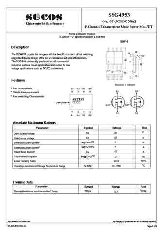
SSG4953 -5A, -30V,RDS(ON) 53m Elektronische Bauelemente P-Channel Enhancement Mode Power Mos.FET RoHS Compliant Product A suffix of "-C" specifies halogen & lead-free SOP-8 Description 0.19 0.25 0.40 0.90 o The SSG4953 provide the designer with the best Combination of fast switching, 0.375 REF ruggedized device design, Ultra low on-resistance and cost-effectiveness. 6.... See More ⇒
tsm4953dcs.pdf
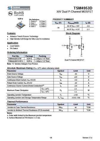
TSM4953D 30V Dual P-Channel MOSFET SOP-8 Pin Definition PRODUCT SUMMARY 1. Source 1 8. Drain 1 2. Gate 1 7. Drain 1 VDS (V) RDS(on)(m ) ID (A) 3. Source 2 6. Drain 2 60 @ VGS = 10V -4.9 4. Gate 2 5. Drain 2 -30 90 @ VGS = 4.5V -3.7 Features Block Diagram Advance Trench Process Technology High Density Cell Design for Ultra Low On-resistance Application ... See More ⇒
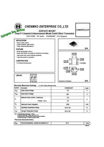
cem4953a.pdf
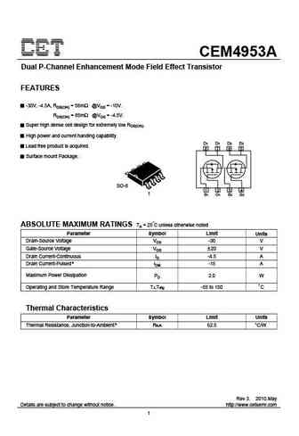
CEM4953A Dual P-Channel Enhancement Mode Field Effect Transistor FEATURES -30V, -4.5A, RDS(ON) = 58m @VGS = -10V. RDS(ON) = 85m @VGS = -4.5V. Super high dense cell design for extremely low RDS(ON). High power and current handing capability. D1 D1 D2 D2 Lead free product is acquired. 8 7 6 5 Surface mount Package. SO-8 1 2 3 4 1 S1 G1 S2 G2 ABSOLUTE MAXIMUM RATINGS TA = 25 ... See More ⇒
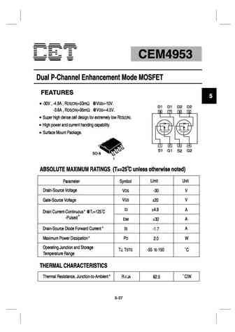
cem4953h.pdf
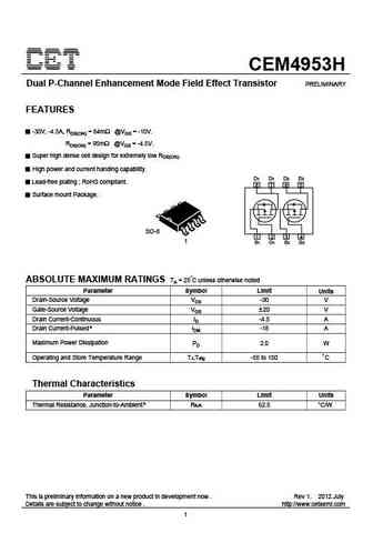
CEM4953H Dual P-Channel Enhancement Mode Field Effect Transistor PRELIMINARY FEATURES -30V, -4.5A, RDS(ON) = 64m @VGS = -10V. RDS(ON) = 95m @VGS = -4.5V. Super high dense cell design for extremely low RDS(ON). High power and current handing capability. D1 D1 D2 D2 Lead-free plating ; RoHS compliant. 8 7 6 5 Surface mount Package. SO-8 1 2 3 4 1 S1 G1 S2 G2 ABSOLUTE MAXIMUM... See More ⇒
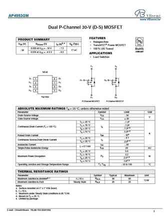
ap4953gm-hf.pdf
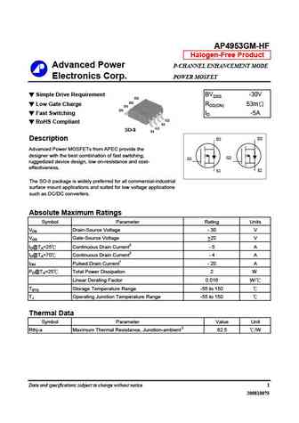
AP4953GM-HF Halogen-Free Product Advanced Power P-CHANNEL ENHANCEMENT MODE Electronics Corp. POWER MOSFET Simple Drive Requirement BVDSS -30V D2 D2 Low Gate Charge RDS(ON) 53m D1 D1 Fast Switching ID -5A G2 RoHS Compliant S2 G1 SO-8 S1 D2 Description D1 Advanced Power MOSFETs from APEC provide the designer with the best combination of fast switching, G2 G... See More ⇒
ap4953gm.pdf
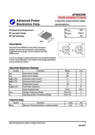
AP4953GM RoHS-compliant Product Advanced Power P-CHANNEL ENHANCEMENT MODE Electronics Corp. POWER MOSFET Simple Drive Requirement BVDSS -30V D2 D2 Low Gate Charge RDS(ON) 53m D1 D1 Fast Switching ID -5A G2 S2 G1 SO-8 S1 D2 Description D1 Advanced Power MOSFETs from APEC provide the designer with the best combination of fast switching, G2 G1 ruggedized device ... See More ⇒
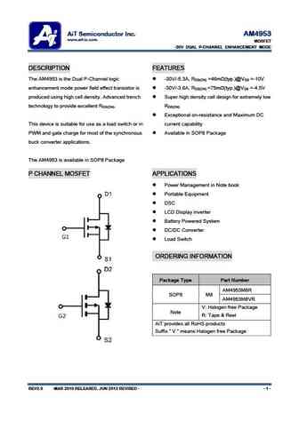
am4953p.pdf
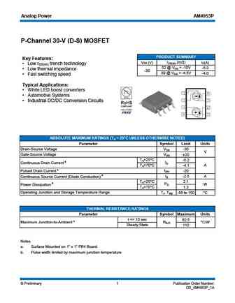
Analog Power AM4953P P-Channel 30-V (D-S) MOSFET PRODUCT SUMMARY Key Features rDS(on) (m ) VDS (V) ID(A) Low r trench technology DS(on) 52 @ VGS = -10V -5.2 Low thermal impedance -30 89 @ VGS = -4.5V -4.0 Fast switching speed Typical Applications White LED boost converters Automotive Systems Industrial DC/DC Conversion Circuits ABSOLUTE MAXIMU... See More ⇒
afp4953s.pdf
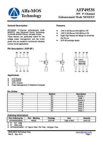
AFP4953S Alfa-MOS 30V P-Channel Technology Enhancement Mode MOSFET General Description Features AFP4953S, P-Channel enhancement mode -30V/-5.4A,RDS(ON)=52m @VGS=10V MOSFET, uses Advanced Trench Technology -30V/-4.2A,RDS(ON)=76m @VGS=4.5V to provide excellent RDS(ON), low gate charge. Super high density cell design for extremely These devices are particularly suite... See More ⇒
afp4953ws.pdf
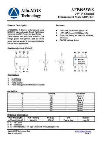
AFP4953WS Alfa-MOS 30V P-Channel Technology Enhancement Mode MOSFET General Description Features AFS4953WS, P-Channel enhancement mode -30V/-5.4A,RDS(ON)=60m @VGS=10V MOSFET, uses Advanced Trench Technology -30V/-4.2A,RDS(ON)=80m @VGS=4.5V to provide excellent RDS(ON), low gate charge. Super high density cell design for extremely These devices are particularly sui... See More ⇒
4953a.pdf

Shenzhen Tuofeng Semiconductor Technology Co., Ltd 4953A 4953A Dual 30V P-Channel PowerTrench MOSFET General Description Features This P MOSFET is a rugged gate version of -Channel 5.3 A, 30 V R = 55 m @ V = 10 V DS(ON) GS Fairchild Semiconductor s advanced PowerTrench R = 85 m @ V = 4.5 V DS(ON) GS process. It has been optimized for power managemen... See More ⇒
4953b.pdf
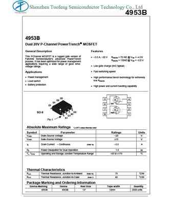
Shenzhen Tuofeng Semiconductor Technology Co., Ltd 4953B 4953B Dual 20V P-Channel PowerTrench MOSFET General Description Features This P MOSFET is a rugged gate version of -Channel 3.5 A, 20 V R = 70 m @ V = 4.5V DS(ON) GS Fairchild Semiconductor s advanced PowerTrench R = 135m @ V = 2.5 .5 V DS(ON) GS process. It has been optimized for power manage... See More ⇒
mtdp4953q8.pdf
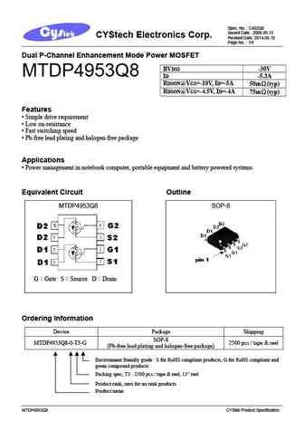
Spec. No. C402Q8 Issued Date 2006.06.15 CYStech Electronics Corp. Revised Date 2014.06.10 Page No. 1/8 Dual P-Channel Enhancement Mode Power MOSFET BVDSS -30V MTDP4953Q8 ID -5.3A RDSON@VGS=-10V, ID=-5A 50m (typ) RDSON@VGS=-4.5V, ID=-4A 75m (typ) Features Simple drive requirement Low on-resistance Fast switching speed Pb-free lead plating and ... See More ⇒
mtdp4953bdyq8.pdf
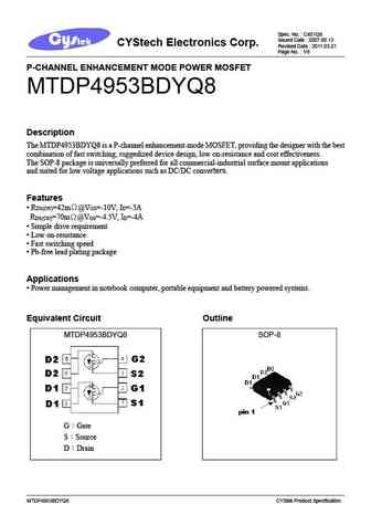
Spec. No. C401Q8 Issued Date 2007.06.13 CYStech Electronics Corp. Revised Date 2011.03.21 Page No. 1/8 P-CHANNEL ENHANCEMENT MODE POWER MOSFET MTDP4953BDYQ8 Description The MTDP4953BDYQ8 is a P-channel enhancement-mode MOSFET, providing the designer with the best combination of fast switching, ruggedized device design, low on-resistance and cost effectiveness. The SO... See More ⇒
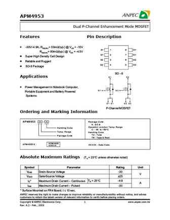
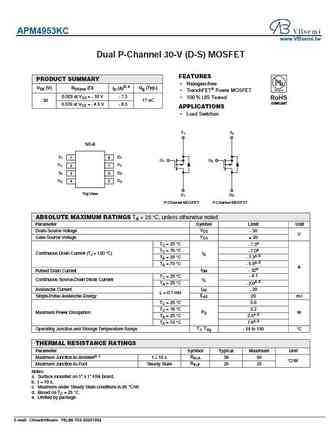
apm4953k.pdf

APM4953K Dual P-Channel Enhancement Mode MOSFET Features Pin Description D1 D1 -30V/-4.9A , D2 D2 RDS(ON)=53m (typ.) @ VGS=-10V RDS(ON)=80m (typ.) @ VGS=-4.5V S1 Reliable and Rugged G1 S2 G2 ESD Protection Top View of SOP 8 Lead Free and Green Devices Available (RoHS Compliant) (1) (3) S1 S2 Applications (2) (4) G1 G2 Power Management in Notebook Computer, Po... See More ⇒
apm4953.pdf
APM4953 Dual P-Channel Enhancement Mode MOSFET Features Pin Description -30V/-4.9A, RDS(ON) = 53m (typ.) @ VGS = -10V S1 1 8 D1 RDS(ON) = 80m (typ.) @ VGS = -4.5V G1 2 7 D1 Super High Density Cell Design S2 3 6 D2 Reliable and Rugged G2 45 D2 SO-8 Package SO - 8 Applications S1 S2 Power Managemen... See More ⇒
stm4953.pdf
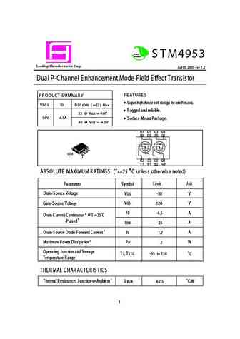
Green Product S TM4953 S amHop Microelectronics C orp. J ul 05 2005 ver 1.2 Dual P-Channel E nhancement Mode Field E ffect Transistor PR ODUC T S UMMAR Y F E ATUR E S S uper high dense cell design for low R DS (ON). VDS S ID R DS (ON) ( m ) Max R ugged and reliable. 55 @ VG S = -10V -30V -4.5A S urface Mount Package. 85 @ VG S = -4.5V D1 D1 D2 D2 8 7 6 5 S O-8 1 1 2 3 4 S... See More ⇒
ssf4953.pdf
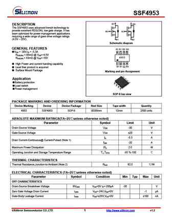
SSF4953 D1 D2 DESCRIPTION The SSF4953 uses advanced trench technology to provide excellent RDS(ON), low gate charge. It has G1 G2 been optimized for power management applications requiring a wide range of gave drive voltage ratings (4.5V 25V). S1 S2 Schematic diagram GENERAL FEATURES D1 D1 D2 D2 VDS = -30V,ID = -5.3A 7 6 5 8 RDS(ON) ... See More ⇒
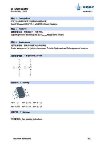
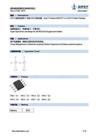
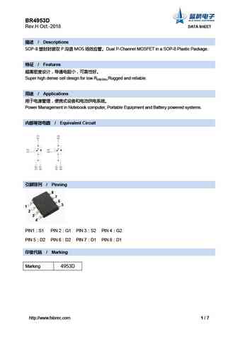
br4953d.pdf
BR4953D Rev.H Oct.-2018 DATA SHEET / Descriptions SOP-8 P MOS Dual P-Channel MOSFET in a SOP-8 Plastic Package. / Features Super high dense cell design for low RDS(ON),Rugged and reliable. / Applications ... See More ⇒
sm4953k.pdf
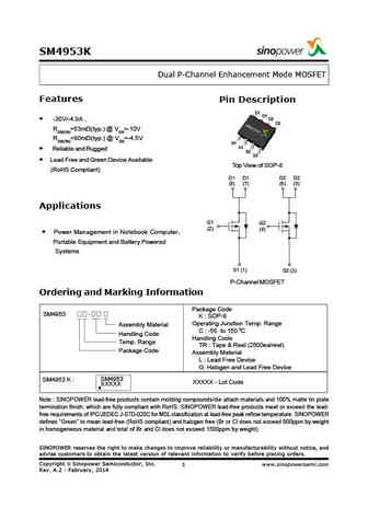
SM4953K Dual P-Channel Enhancement Mode MOSFET Features Pin Description D1 D1 D2 -30V/-4.9A , D2 RDS(ON)=53m (typ.) @ VGS=-10V RDS(ON)=80m (typ.) @ VGS=-4.5V S1 G1 Reliable and Rugged S2 G2 Lead Free and Green Device Available Top View of SOP-8 (RoHS Compliant) D1 D1 D2 D2 (8) (7) (6) (5) Applications G1 G2 (2) (4) Power Management in Notebook Computer, Portable... See More ⇒
apm4953k.pdf
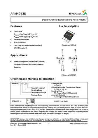
APM4953K Dual P-Channel Enhancement Mode MOSFET Features Pin Description D1 D1 -30V/-4.9A , D2 D2 RDS(ON)=53m (typ.) @ VGS=-10V RDS(ON)=80m (typ.) @ VGS=-4.5V S1 Reliable and Rugged G1 S2 G2 ESD Protection Top View of SOP 8 Lead Free and Green Devices Available (RoHS Compliant) (1) (3) S1 S2 Applications (2) (4) G1 G2 Power Management in Notebook Computer, Po... See More ⇒
ftk4953.pdf
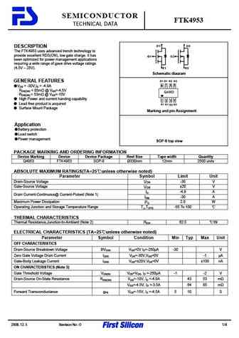
SEMICONDUCTOR FTK4953 TECHNICAL DATA D1 D2 DESCRIPTION The FTK4953 uses advanced trench technology to provide excellent RDS(ON), low gate charge. It has G1 G2 been optimized for power management applications requiring a wide range of gave drive voltage ratings (4.5V 25V). S1 S2 Schematic diagram GENERAL FEATURES D 1 D 1 D2 D 2 8 7 6 5 VDS = -30V,ID = -4.9A RDS(ON) ... See More ⇒
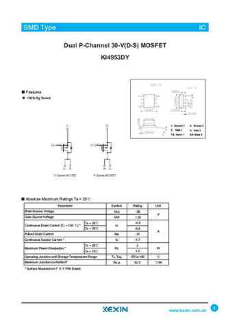
ki4953dy.pdf
SMD Type IC SMD Type IC Dual P-Channel 30-V(D-S) MOSFET KI4953DY Features 100% Rg Tested 1 Source 1 3 Source 2 2 Gate 1 4 Gate 2 7,8 Drain 1 5,6 Drain 2 Absolute Maximum Ratings Ta = 25 Parameter Symbol Rating Unit Drain-Source Voltage VDS -30 V Gate-Source Voltage VGS 20 TA =25 -4.9 Continuous Drain Current (TJ = 150 ) * ID TA =70 -3.9 A Pulsed Drain Current IDM -30 C... See More ⇒
kds4953.pdf
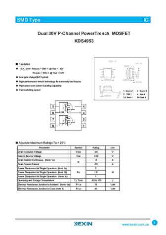
SMD Type IC SMD Type IC Dual 30V P-Channel PowerTrench MOSFET KDS4953 Features -5 A, -30 V. RDS(ON) = 55m @VGS = -10V RDS(ON) = 95m @VGS =-4.5V Low gate charge(6nC typical) High performance trench technology for extremely low RDS(ON) High power and current handling capability Fast switching speed 1 Source 1 3 Source 2 2 Gate 1 4 Gate 2 7,8 Drain 1 5,6 Drain 2 Absolute Maxim... See More ⇒
si4953ady.pdf
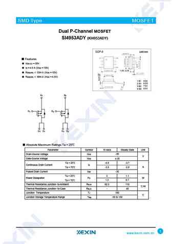
SMD Type MOSFET Dual P-Channel MOSFET SI4953ADY (KI4953ADY) SOP-8 Unit mm Features VDS (V) =-30V ID =-4.9 A (VGS =-10V) 1.50 0.15 RDS(ON) 53m (VGS =-10V) RDS(ON) 90m (VGS =-4.5V) 1 S1 5 D2 6 D2 2 G1 7 D1 3 S2 8 D1 4 G2 S1 S2 G1 G2 D1 D1 D2 D2 Absolute Maximum Ratings Ta = 25 Parameter Symbol 10 secs Steady State Unit Drain-Sourc... See More ⇒
si4953dy.pdf
SMD Type MOSFET Dual P-Channel MOSFET SI4953DY (KI4953DY) SOP-8 Features VDS (V) =-30V ID =-4.9 A (VGS =-10V) 1.50 0.15 RDS(ON) 53m (VGS =-10V) RDS(ON) 95m (VGS =-4.5V) 1 Source1 5 Drain2 6 Drain2 2 Gate1 7 Drain1 3 Source2 S1 S2 8 Drain1 4 Gate2 G1 G2 D1 D1 D2 D2 Absolute Maximum Ratings Ta = 25 Parameter Symbol Rating Unit Drai... See More ⇒
am4953.pdf
AiT Semiconductor Inc. AM4953 www.ait-ic.com MOSFET -30V DUAL P-CHANNEL ENHANCEMENT MODE DESCRIPTION FEATURES The AM4953 is the Dual P-Channel logic -30V/-5.3A, R =46m (typ.)@V =-10V DS(ON) GS enhancement mode power field effect transistor is -30V/-3.6A, R =75m (typ.)@V =-4.5V DS(ON) GS produced using high cell density. Advanced trench Super high density cell desig... See More ⇒
blm4953.pdf
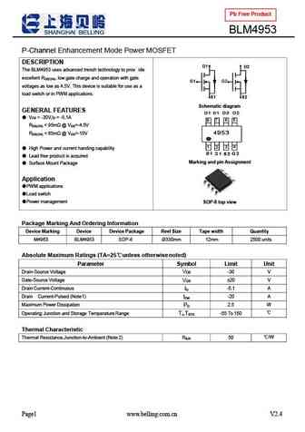
Pb Free Product BLM4953 P-Channel Enhancement Mode Power MOSFET DESCRIPTION D 1 D 2 The BLM4953 uses advanced trench technology to prov ide excellent R , low gate charge and operation with gate DS(ON) G 1 G 2 voltages as low as 4.5V. This device is suitable for use as a load switch or in PWM applications. S 1 S 2 Schematic diagram GENERAL FEATURES VDS = -30V,ID ... See More ⇒
blm4953a.pdf

Pb Free Product BLM4953A P-Channel Enhancement Mode Power MOSFET DESCRIPTION D1 D2 The BLM4953A uses advanced trench technology to provide excellent R , low gate charge and operation with gate DS(ON) G1 G2 voltages as low as 4.5V. This device is suitable for use as a load switch or in PWM applications. S1 S2 Schematic diagram GENERAL FEATURES V = -30V,I = -5.3A DS... See More ⇒
chm4953jgp.pdf
CHENMKO ENTERPRISE CO.,LTD CHM4953JGP SURFACE MOUNT Dual P-Channel Enhancement Mode Field Effect Transistor VOLTAGE 30 Volts CURRENT 4.9 Ampere APPLICATION * Servo motor control. * Power MOSFET gate drivers. * Other switching applications. SO-8 FEATURE * Small flat package. (SO-8 ) ( ) * Super high dense cell design for extremely low RDS(ON). 4.06 0.160 ( ) 3.70 0.146 * High ... See More ⇒
gsm4953s.pdf
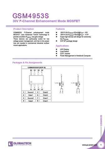
30V P-Channel Enhancement Mode MOSFET Product Description Features GSM4953S, P-Channel enhancement mode -30V/-5.4A,RDS(ON)=52m @VGS= -10V MOSFET, uses Advanced Trench Technology to -30V/-4.2A,RDS(ON)=76m @VGS= - 4.5V provide excellent RDS(ON), low gate charge. Super high density cell design for extremely These devices are particularly suited for low low RDS (ON) volt... See More ⇒
gsm4953ws.pdf
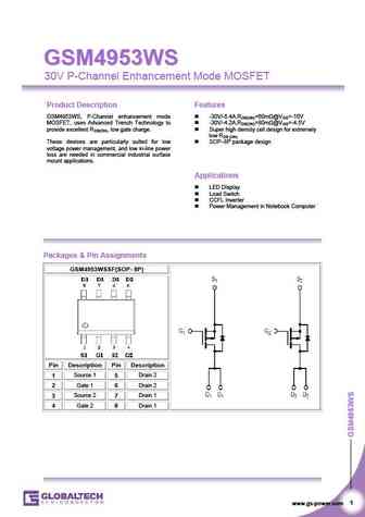
GSM4953WS GSM4953WS 30V P-Channel Enhancement Mode MOSFET Product Description Features GSM4953WS, P-Channel enhancement mode -30V/-5.4A,RDS(ON)=60m @VGS=-10V MOSFET, uses Advanced Trench Technology to -30V/-4.2A,RDS(ON)=80m @VGS=-4.5V provide excellent RDS(ON), low gate charge. Super high density cell design for extremely low RDS (ON) These devices are particula... See More ⇒
mt4953.pdf
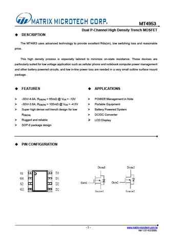
MT4953 Dual P-Channel High Density Trench MOSFET DESCRIPTION The MT4953 uses advanced technology to provide excellent Rds(on), low switching loss and reasonable price. This high density process is especially tailored to minimize on-state resistance. These devices are particularly suited for low voltage application such as cellular phone and notebook computer power management and ... See More ⇒
me4953 me4953-g.pdf
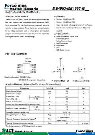
ME4953/ME4953-G Dual P-Channel 30V (D-S) MOSFET GENERAL DESCRIPTION FEATURES RDS(ON) 60m @VGS=-10V The ME4953 is the Dual P-Channel logic enhancement mode power RDS(ON) 90m @VGS=-4.5V field effect transistors are produced using high cell density, DMOS Super high density cell design for extremely low RDS(ON) trench technology. This high density process is espec... See More ⇒
nce4953.pdf
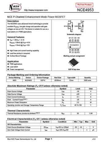
Pb Free Product http //www.ncepower.com NCE4953 NCE P-Channel Enhancement Mode Power MOSFET Description D1 D2 The NCE4953 uses advanced trench technology to provide G1 G2 excellent RDS(ON), low gate charge and operation with gate voltages as low as 4.5V. This device is suitable for use as a S1 S2 load switch or in PWM applications. Schematic diagram General Features VD... See More ⇒
ps4953a.pdf
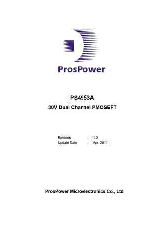
PS4953A 30V Dual Channel PMOSEFT Revision 1.0 Update Date Apr. 2011 ProsPower Microelectronics Co., Ltd PS4953A 30V Dual Channel PMOSFET 2. Applications 1. General Description PWM applications The PS4953A uses advanced trench technology Load switch and design to provide excellent Rds(on) with low Power management gate charge and operation with gate voltages as ... See More ⇒
stp4953a.pdf
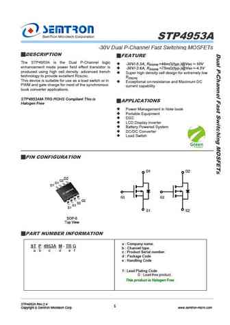
STP4953A -30V Dual P-Channel Fast Switching MOSFETs DESCRIPTION FEATURE The STP4953A is the Dual P-Channel logic -30V/-5.3A, RDS(ON) =46m (typ.)@VGS =-10V enhancement mode power field effect transistor is -30V/-3.6A, RDS(ON) =75m (typ.)@VGS =-4.5V produced using high cell density. advanced trench Super high density cell design for extremely low technology ... See More ⇒
ssm4953m.pdf
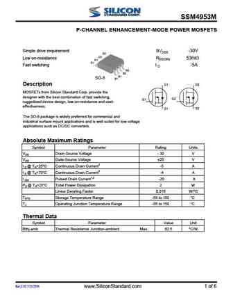
SSM4953M P-CHANNEL ENHANCEMENT-MODE POWER MOSFETS Simple drive requirement BVDSS -30V D2 D2 Low on-resistance RDS(ON) 53m D1 D1 Fast switching I -5A D G2 S2 G1 SO-8 S1 D2 Description D1 MOSFETs from Silicon Standard Corp. provide the designer with the best combination of fast switching, G2 G1 ruggedized device design, low on-resistance and cost- effectiveness. S2 S1 ... See More ⇒
stp4953.pdf
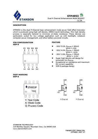
STP4953 Dual P Channel Enhancement Mode MOSFET -5.2A DESCRIPTION STP4953 is the dual P-Channel logic enhancement mode power field effect transistor which is produced using high cell density, DMOS trench technology. This high density process is especially tailored to minimize on-state resistance. These devices are particularly suited for low voltage application such as LCD backli... See More ⇒
ec4953.pdf
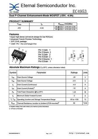
Eternal Semiconductor Inc. EC4953 Dual P-Channel Enhancement-Mode MOSFET (-20V, -4.8A) PRODUCT SUMMARY VDSS ID RDS(on) (m )Max 85 @VGS = -2.5V,ID=-2.0A -20V -4.8A 64 @VGS = -4.5V,ID=-4.8A Features Super high dense cell trench design for low RDS(on) Advanced Trench Process Technology SOT-23-6L package Lead Pb -free and halogen-free 6 Pin 1 Gate 1 5 4 Pin 2... See More ⇒
es4953.pdf
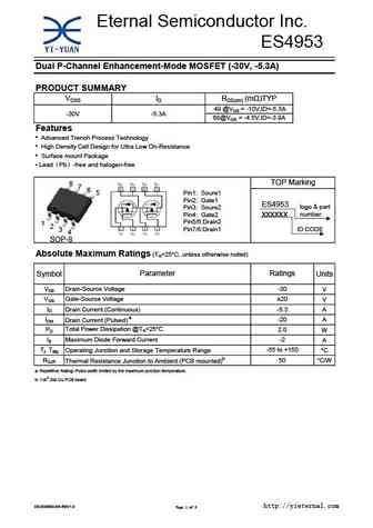
Eternal Semiconductor Inc. ES4953 Dual P-Channel Enhancement-Mode MOSFET (-30V, -5.3A) PRODUCT SUMMARY VDSS ID RDS(on) (m )TYP 49 @VGS = -10V,ID=-5.3A -30V -5.3A 68@VGS = -4.5V,ID=-3.9A Features Advanced Trench Process Technology High Density Cell Design for Ultra Low On-Resistance Surface mount Package Lead Pb -free and halogen-free TOP Marking 8 7 6 5 P... See More ⇒
gm4953.pdf
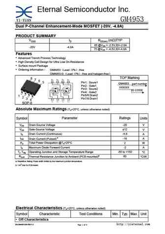
Eternal Semiconductor Inc. GM4953 Dual P-Channel Enhancement-Mode MOSFET (-20V, -4.8A) PRODUCT SUMMARY VDSS ID RDS(on) (m )TYP 85 @VGS = -2.5V,ID=-2.0A -20V -4.8A 75 @VGS = -4.5V,ID=-4.8A Features Advanced Trench Process Technology High Density Cell Design for Ultra Low On-Resistance Surface mount Package Ordering information GM4953 Lead Pb -free GM4953... See More ⇒
2n4265 2n4400 2n4401 2n4402 2n4403 2n4409 2n4410 2n4424 2n4425 2n4951 2n4952 2n4953 2n4954 2n5087 2n5088 2n5089.pdf
... See More ⇒
jmtp4953b.pdf
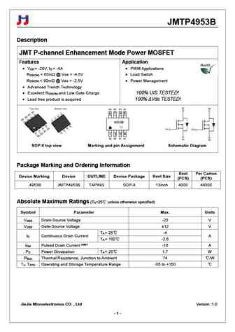
JMTP4953B Description JMT P-channel Enhancement Mode Power MOSFET Features Application V = -20V, I = -4A PWM Applications DS D R ... See More ⇒
jmtp4953a.pdf
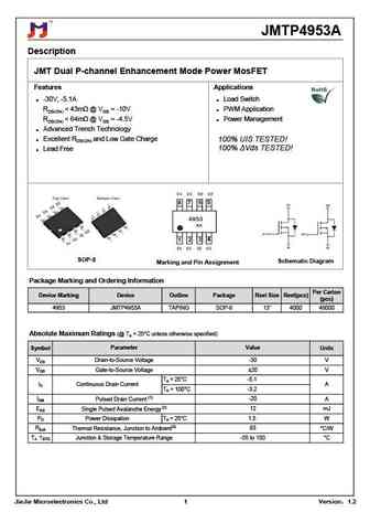
JMTP4953A Description JMT Dual P-channel Enhancement Mode Power MosFET Features Applications -30V, -5.1A Load Switch RDS(ON) ... See More ⇒
jsm4953.pdf
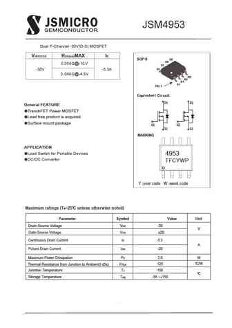
JSM4953 Dual P-Channel -30V(D-S) MOSFET V(BR)DSS RDS(on)MAX ID SOP-8 D2 D2 0.059 @-10V . D1 -30V -5.3A D1 0.089 @-4.5V G2 G S2 G1 S S S1 SO-8 S Pin 1 Equivalent Cir cuit D1 D2 General FEATURE TrenchFET Power MOSFET Lead free product is acquired Surface mount package G1 G2 S1 S2 MARKING APPLICATION Load Switch for Portable Devices 4953 DC/DC Conv... See More ⇒
lpm4953.pdf
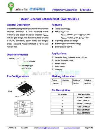
Preliminary Datasheet LPM4953 Dual P -Channel Enhancement Power MOSFET General Description Features The LPM4953 integrates two P-Channel enhancement Trench Technology MOSFET Transistor. It uses advanced trench PMOS V =-15V DS technology and design to provide excellent R R ... See More ⇒
pt4953.pdf
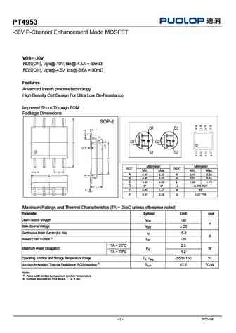
PT4953 -30V P-Channel Enhancement Mode MOSFET VDS= -30V RDS(ON), Vgs@-10V, Ids@-4.5A = 63m RDS(ON), Vgs@-4.5V, Ids@-3.6A = 90m Features Advanced trench process technology High Density Cell Design For Ultra Low On-Resistance Improved Shoot-Through FOM Package Dimensions D1 D1 D2 D2 8 7 6 5 1 2 3 4 S1 G1 S2 G2 Millimeter Millimeter REF. REF. Min. Max. Min. Max. A ... See More ⇒
4953b.pdf
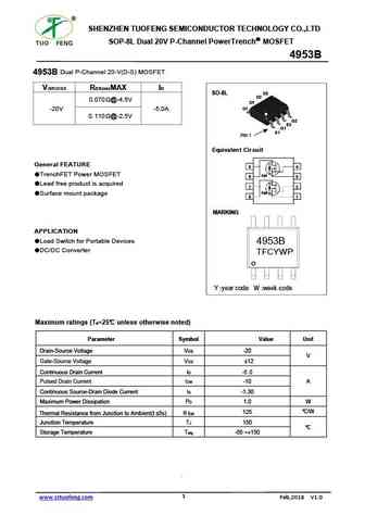
SHENZHEN TUOFENG SEMICONDUCTOR TECHNOLOGY CO.,LTD SOP-8L Dual 20V P-Channel PowerTrench MOSFET 4953B Dual P-Channel 20-V(D-S) MOSFET 4953B V(BR)DSS RDS(on)MAX ID SO-8L D2 D2 0.070 @-4.5V D1 -20V -5.0A D1 0.110 @-2.5V G2 G S2 G1 S S S1 SO-8 S Pin 1 Equivalent Cir cuit General FEATURE 5 4 TrenchFET Power MOSFET Q1 6 3 Lead free product is acquired 7 2 Q2 S... See More ⇒
wsp4953a.pdf
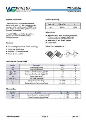
WSP4953A Dual P-Ch MOSFET General Description Product Summery The WSP4953A is the highest performance BVDSS RDSON ID trench P-ch MOSFETs with extreme high cell density , which provide excellent RDSON and -20V 40m -5.8A gate charge for most of the synchronous buck converter applications . Applications The WSP4953A meet the RoHS and Green Product requirement with full fu... See More ⇒
wsp4953.pdf
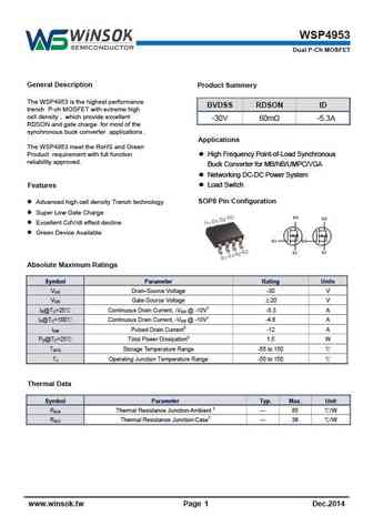
WSP4953 Dual P-Ch MOSFET General Description Product Summery The WSP4953 is the highest performance BVDSS RDSON ID trench P-ch MOSFET with extreme high cell density , which provide excellent -30V 60m -5.3A RDSON and gate charge for most of the synchronous buck converter applications . Applications The WSP4953 meet the RoHS and Green Product requirement with full functi... See More ⇒
se4953.pdf
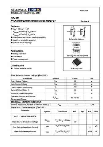
SHANGHAI June 2006 MICROELECTRONICS CO., LTD. SE4953 P-Channel Enhancement-Mode MOSFET Revision A Features VDS = -30V,ID = -4.9A RDS(ON) ... See More ⇒
sm4953.pdf
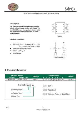
SM4953 Dual P-Channel Enhancement Mode MOSFET Description The SM4953 uses advanced trench technology to provide excellent RDS(ON) and low gate charge. The two MOSFETs make a compact and efficient switch and synchronous rectifier combination for use in buck converters. SOIC-8 General Features Ordering Information Ordering Number Pin Assignment Package Packi... See More ⇒
gt4953.pdf

GT4953 www.VBsemi.tw Dual P-Channel 30-V (D-S) MOSFET FEATURES PRODUCT SUMMARY Halogen-free VDS (V) RDS(on) ( ) ID (A)d, e Qg (Typ.) TrenchFET Power MOSFET 0.029 at VGS = - 10 V - 7.3 100 % UIS Tested RoHS - 30 17 nC COMPLIANT 0.039 at VGS = - 4.5 V - 6.3 APPLICATIONS Load Switches S1 S2 SO-8 S1 1 D1 8 G1 G2 G1 2 D1 7 S2 3 D2 6 G2 4 D2 5 Top View ... See More ⇒
si4953ady-t1-e3.pdf
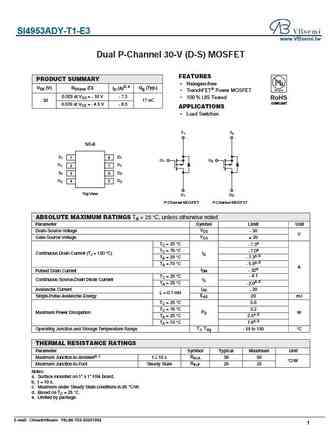
SI4953ADY-T1-E3 www.VBsemi.tw Dual P-Channel 30-V (D-S) MOSFET FEATURES PRODUCT SUMMARY Halogen-free VDS (V) RDS(on) ( ) ID (A)d, e Qg (Typ.) TrenchFET Power MOSFET 0.029 at VGS = - 10 V - 7.3 100 % UIS Tested RoHS - 30 17 nC COMPLIANT 0.039 at VGS = - 4.5 V - 6.3 APPLICATIONS Load Switches S1 S2 SO-8 S1 1 D1 8 G1 G2 G1 2 D1 7 S2 3 D2 6 G2 4 D2 5 ... See More ⇒
kd4953.pdf
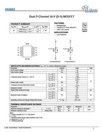
KD4953 www.VBsemi.tw Dual P-Channel 30-V (D-S) MOSFET FEATURES PRODUCT SUMMARY Halogen-free VDS (V) RDS(on) ( ) ID (A)d, e Qg (Typ.) TrenchFET Power MOSFET 0.029 at VGS = - 10 V - 7.3 100 % UIS Tested RoHS - 30 17 nC COMPLIANT 0.039 at VGS = - 4.5 V - 6.3 APPLICATIONS Load Switches S1 S2 SO-8 S1 1 D1 8 G1 G2 G1 2 D1 7 S2 3 D2 6 G2 4 D2 5 Top View ... See More ⇒
nce4953.pdf

NCE4953 www.VBsemi.tw Dual P-Channel 30-V (D-S) MOSFET FEATURES PRODUCT SUMMARY Halogen-free VDS (V) RDS(on) ( ) ID (A)d, e Qg (Typ.) TrenchFET Power MOSFET 0.029 at VGS = - 10 V - 7.3 100 % UIS Tested RoHS - 30 17 nC COMPLIANT 0.039 at VGS = - 4.5 V - 6.3 APPLICATIONS Load Switches S1 S2 SO-8 S1 1 D1 8 G1 G2 G1 2 D1 7 S2 3 D2 6 G2 4 D2 5 Top View... See More ⇒
ap4953m.pdf

AP4953M www.VBsemi.tw Dual P-Channel 30-V (D-S) MOSFET FEATURES PRODUCT SUMMARY Halogen-free VDS (V) RDS(on) ( ) ID (A)d, e Qg (Typ.) TrenchFET Power MOSFET 0.029 at VGS = - 10 V - 7.3 100 % UIS Tested RoHS - 30 17 nC COMPLIANT 0.039 at VGS = - 4.5 V - 6.3 APPLICATIONS Load Switches S1 S2 SO-8 S1 1 D1 8 G1 G2 G1 2 D1 7 S2 3 D2 6 G2 4 D2 5 Top View... See More ⇒
sdm4953a.pdf

SDM4953A www.VBsemi.tw Dual P-Channel 30-V (D-S) MOSFET FEATURES PRODUCT SUMMARY Halogen-free VDS (V) RDS(on) ( ) ID (A)d, e Qg (Typ.) TrenchFET Power MOSFET 0.029 at VGS = - 10 V - 7.3 100 % UIS Tested RoHS - 30 17 nC COMPLIANT 0.039 at VGS = - 4.5 V - 6.3 APPLICATIONS Load Switches S1 S2 SO-8 S1 1 D1 8 G1 G2 G1 2 D1 7 S2 3 D2 6 G2 4 D2 5 Top Vie... See More ⇒
vbza4953a.pdf
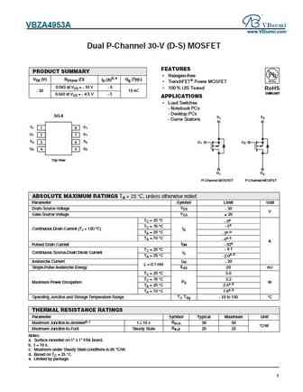
VBZA4953A www.VBsemi.com Dual P-Channel 30-V (D-S) MOSFET FEATURES PRODUCT SUMMARY Halogen-free VDS (V) RDS(on) ( ) ID (A)d, e Qg (Typ.) TrenchFET Power MOSFET 0.040 at VGS = - 10 V - 6 100 % UIS Tested RoHS - 30 15 nC COMPLIANT 0.048 at VGS = - 4.5 V - 5 APPLICATIONS Load Switches - Notebook PCs - Desktop PCs SO-8 S1 S2 - Game Stations S1 1 D1 8 G1 2... See More ⇒
sm4953kc.pdf
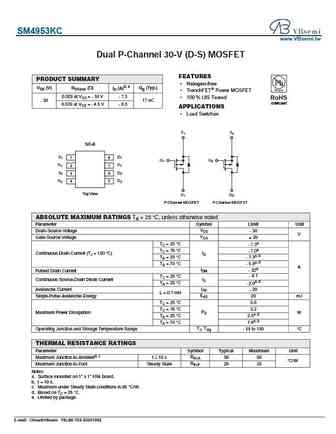
SM4953KC www.VBsemi.tw Dual P-Channel 30-V (D-S) MOSFET FEATURES PRODUCT SUMMARY Halogen-free VDS (V) RDS(on) ( ) ID (A)d, e Qg (Typ.) TrenchFET Power MOSFET 0.029 at VGS = - 10 V - 7.3 100 % UIS Tested RoHS - 30 17 nC COMPLIANT 0.039 at VGS = - 4.5 V - 6.3 APPLICATIONS Load Switches S1 S2 SO-8 S1 1 D1 8 G1 G2 G1 2 D1 7 S2 3 D2 6 G2 4 D2 5 Top Vie... See More ⇒
vbza4953.pdf
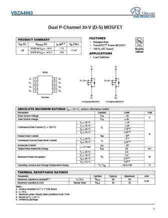
VBZA4953 www.VBsemi.com Dual P-Channel 30-V (D-S) MOSFET FEATURES PRODUCT SUMMARY Halogen-free VDS (V) RDS(on) ( ) ID (A)d, e Qg (Typ.) TrenchFET Power MOSFET 0.029 at VGS = - 10 V - 7.3 100 % UIS Tested RoHS - 30 17 nC COMPLIANT 0.039 at VGS = - 4.5 V - 6.3 APPLICATIONS Load Switches S1 S2 SO-8 S1 1 D1 8 G1 G2 G1 2 D1 7 S2 3 D2 6 G2 4 D2 5 Top Vi... See More ⇒
ap4953gm.pdf
AP4953GM www.VBsemi.tw Dual P-Channel 30-V (D-S) MOSFET FEATURES PRODUCT SUMMARY Halogen-free VDS (V) RDS(on) ( ) ID (A)d, e Qg (Typ.) TrenchFET Power MOSFET 0.029 at VGS = - 10 V - 7.3 100 % UIS Tested RoHS - 30 17 nC COMPLIANT 0.039 at VGS = - 4.5 V - 6.3 APPLICATIONS Load Switches S1 S2 SO-8 S1 1 D1 8 G1 G2 G1 2 D1 7 S2 3 D2 6 G2 4 D2 5 Top Vie... See More ⇒
si4953dy-t1-e3.pdf
SI4953DY-T1-E3 www.VBsemi.tw Dual P-Channel 30-V (D-S) MOSFET FEATURES PRODUCT SUMMARY Halogen-free VDS (V) RDS(on) ( ) ID (A)d, e Qg (Typ.) TrenchFET Power MOSFET 0.029 at VGS = - 10 V - 7.3 100 % UIS Tested RoHS - 30 17 nC COMPLIANT 0.039 at VGS = - 4.5 V - 6.3 APPLICATIONS Load Switches S1 S2 SO-8 S1 1 D1 8 G1 G2 G1 2 D1 7 S2 3 D2 6 G2 4 D2 5 T... See More ⇒
apm4953kc.pdf
APM4953KC www.VBsemi.tw Dual P-Channel 30-V (D-S) MOSFET FEATURES PRODUCT SUMMARY Halogen-free VDS (V) RDS(on) ( ) ID (A)d, e Qg (Typ.) TrenchFET Power MOSFET 0.029 at VGS = - 10 V - 7.3 100 % UIS Tested RoHS - 30 17 nC COMPLIANT 0.039 at VGS = - 4.5 V - 6.3 APPLICATIONS Load Switches S1 S2 SO-8 S1 1 D1 8 G1 G2 G1 2 D1 7 S2 3 D2 6 G2 4 D2 5 Top Vi... See More ⇒
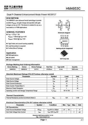
hm4953c.pdf
HM4953C Dual P-Channel Enhancement Mode Power MOSFET DESCRIPTION The HM4953C uses advanced trench technology to provide D D excellent RDS(ON), low gate charge and operation with gate voltages as low as 2.5V. This device is suitable for use as a G G load switch or in PWM applications. S S GENERAL FEATURES Schematic diagram VDS = -27V,ID = -5A RDS(ON) ... See More ⇒
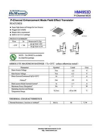
hm4953b.pdf

HM4953B Dual P-Channel Enhancement Mode Power MOSFET DESCRIPTION The HM4953B uses advanced trench technology to provide D D excellent RDS(ON), low gate charge and operation with gate voltages as low as 2.5V. This device is suitable for use as a G G load switch or in PWM applications. S S GENERAL FEATURES Schematic diagram VDS = -20V,ID = -5A RDS(ON) ... See More ⇒
hm4953.pdf

HM4953 Dual P-Channel Enhancement Mode Power MOSFET DESCRIPTION D1 D2 The HM4953 uses advanced trench technology to provide excellent RDS(ON), low gate charge and operation with gate G1 G2 voltages as low as 4.5V. This device is suitable for use as a load switch or in PWM applications. S1 S2 Schematic diagram GENERAL FEATURES VDS = -30V,ID = -5.1A RDS(ON) ... See More ⇒
hm4953a.pdf
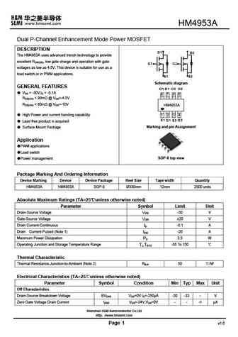
HM4953A Dual P-Channel Enhancement Mode Power MOSFET DESCRIPTION D1 D2 The HM4953A uses advanced trench technology to provide excellent RDS(ON), low gate charge and operation with gate G1 G2 voltages as low as 4.5V. This device is suitable for use as a load switch or in PWM applications. S1 S2 Schematic diagram GENERAL FEATURES VDS = -30V,ID = -5.1A RDS(ON) ... See More ⇒
hm4953d.pdf
Shenzhen H&M Semiconductor Co.Ltd http //www.hmsemi.com Shenzhen H&M Semiconductor Co.Ltd http //www.hmsemi.com Shenzhen H&M Semiconductor Co.Ltd http //www.hmsemi.com Shenzhen H&M Semiconductor Co.Ltd http //www.hmsemi.com ... See More ⇒
2sc4953.pdf
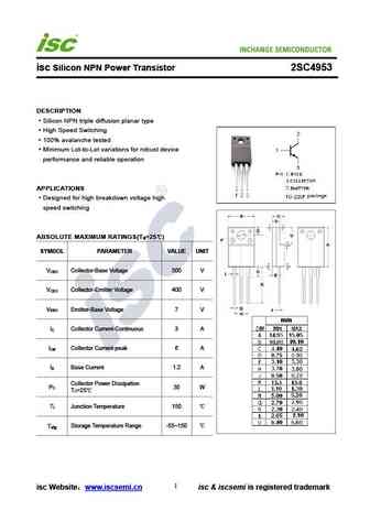
INCHANGE Semiconductor isc Silicon NPN Power Transistor 2SC4953 DESCRIPTION Silicon NPN triple diffusion planar type High Speed Switching 100% avalanche tested Minimum Lot-to-Lot variations for robust device performance and reliable operation APPLICATIONS Designed for high breakdown voltage high speed switching ABSOLUTE MAXIMUM RATINGS(T =25 ) a SYMBOL PARAMETER VALUE U... See More ⇒
ap4953b.pdf
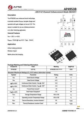
AP4953B -20V P+P-Channel Enhancement Mode MOSFET Description The AP4953B uses advanced trench technology to provide excellent R , low gate charge and DS(ON) operation with gate voltages as low as 4.5V. This device is suitable for use as a Battery protection or in other Switching application. General Features V = -20V I =-6.5A DS D R ... See More ⇒
ap4953a.pdf
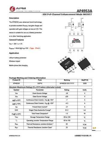
AP4953A -30V P+P-Channel Enhancement Mode MOSFET Description The AP4953A uses advanced trench technology to provide excellent R , low gate charge and DS(ON) operation with gate voltages as low as 4.5V. This device is suitable for use as a Battery protection or in other Switching application. General Features V = -30V I =-7A DS D R ... See More ⇒
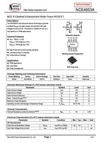
Detailed specifications: 4612 , 4616 , 4622 , 4803 , 4812 , 4835 , 4920 , 4946 , AON7410 , 6604 , 8810 , 8820 , 8822 , 9435 , 4953A , 4953B , 9926A .
History: AUIRF1010EZ
Keywords - 4953 MOSFET specs
4953 cross reference
4953 equivalent finder
4953 pdf lookup
4953 substitution
4953 replacement
Learn how to find the right MOSFET substitute. A guide to cross-reference, check specs and replace MOSFETs in your circuits.
History: AUIRF1010EZ
🌐 : EN ES РУ

LIST
Last Update
MOSFET: ASB80R750E | ASB70R380E | ASB65R300E | ASB65R220E | ASB65R120EFD | ASB60R150E | ASA80R900E | ASA80R750E | ASA80R290E | ASA70R950E
Popular searches
c1096 transistor | c1345 transistor | jcs640c | kn2907a | ncep028n85 datasheet | sw50n06 | 2sa1232 | 2sc1940