9435 Specs and Replacement
Type Designator: 9435
Type of Transistor: MOSFET
Type of Control Channel: P-Channel
Absolute Maximum Ratings
Pd ⓘ - Maximum Power Dissipation: 2.5 W
|Vds|ⓘ - Maximum Drain-Source Voltage: 30 V
|Vgs|ⓘ - Maximum Gate-Source Voltage: 20 V
|Id| ⓘ - Maximum Drain Current: 5.3 A
Tj ⓘ - Maximum Junction Temperature: 150 °C
Electrical Characteristics
RDSonⓘ - Maximum Drain-Source On-State Resistance: 0.06 Ohm
Package: SOP8
9435 substitution
- MOSFET ⓘ Cross-Reference Search
9435 datasheet
9435.pdf
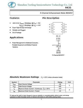
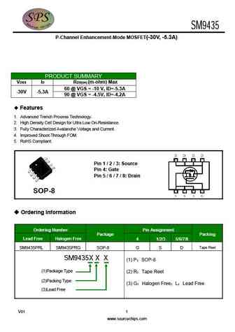
Shenzhen Tuofeng Semiconductor Technology Co., Ltd 9435 P-Channel Enhancement Mode MOSFET Features Pin Description -30V/-5.3A, RDS(ON) = 60m (typ.) @ VGS = -10V S 1 8 D RDS(ON) = 90m (typ.) @ VGS = -4.5V S 2 7 D Super High Density Cell Design S 3 6 D Reliable and Rugged G 45 D SO-8 Package SO - 8 Ap... See More ⇒
9435.pdf
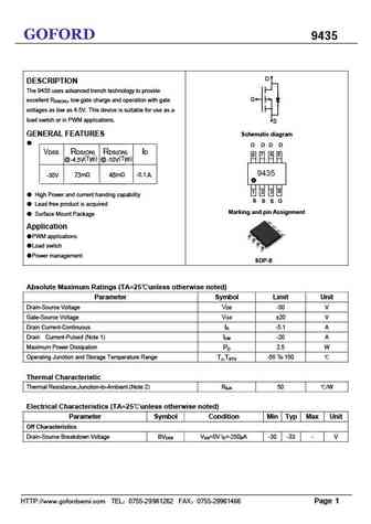
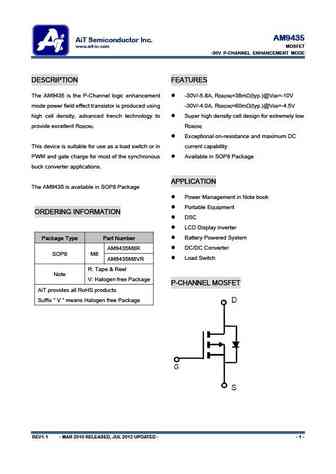
GOFORD 9435 D DESCRIPTION The 9435 uses advanced trench technology to provide G excellent RDS(ON), low gate charge and operation with gate voltages as low as 4.5V. This device is suitable for use as a load switch or in PWM applications. S GENERAL FEATURES Schematic diagram VDSS RDS(ON) RDS(ON) ID @ (Typ) @ -4.5V -10V (Typ) m m -30V 73 48 -5.1 A High Power a... See More ⇒
9435.pdf
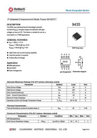
Plastic-Encapsulate Mosfets P-Channel Enhancement Mode Power MOSFET DESCRIPTION 9435 The 9435 uses advanced trench technology to provide excellent RDS(ON), low gate charge and operation with gate voltages as low as 4.5V. This device is suitable for use as a load switch or in PWM applications. GENERAL FEATURES VDS = -30V,ID = -5.1A RDS(ON) ... See More ⇒
9435.pdf
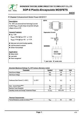
SHENZHEN TUOFENG SEMICONDUCTOR TECHNOLOGY CO.,LTD SOP-8 Plastic-Encapsulate MOSFETS 9435 P-Channel Enhancement Mode Power MOSFET SOP-8 Description SD 1 8 The 9435 uses advanced trench technology to provide S D 2 7 excellent RDS(ON), low gate charge and operation with gate SD 3 6 G D 4 5 voltages as low as 4.5V. Top View Equivalent Cir cuit General Features S VDS ... See More ⇒
mmjt9435.pdf
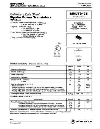
Order this document MOTOROLA by MMJT9435/D SEMICONDUCTOR TECHNICAL DATA MMJT9435 Preliminary Data Sheet Motorola Preferred Device Bipolar Power Transistors PNP Silicon Collector Emitter Sustaining Voltage VCEO(sus) POWER BJT = 30 Vdc (Min) @ IC = 10 mAdc IC = 3.0 AMPERES High DC Current Gain hFE BVCEO = 30 VOLTS = 140 (Min) @ IC = 1.2 Adc VCE(sat) = 0.275 VOLTS... See More ⇒
fds9435a.pdf
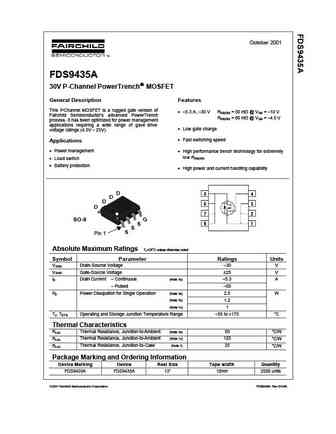
October 2001 FDS9435A 30V P-Channel PowerTrench MOSFET General Description Features This P MOSFET is a rugged gate version of -Channel 5.3 A, 30 V R = 50 m @ V = 10 V DS(ON) GS Fairchild Semiconductor s advanced PowerTrench R = 80 m @ V = 4.5 V DS(ON) GS process. It has been optimized for power management applications requiring a wide range of gave... See More ⇒
nds9435a.pdf

January 2002 NDS9435A 30V P-Channel PowerTrench MOSFET General Description Features This P-Channel MOSFET is a rugged gate version of 5.3 A, 30 V RDS(ON) = 50 m @ VGS = 10 V Fairchild Semiconductor s advanced PowerTrench RDS(ON) = 80 m @ VGS = 4.5 V process. It has been optimized for power management applications requiring a wide rang... See More ⇒
dmjt9435.pdf
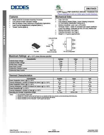
DMJT9435 LOW VCE(SAT) PNP SURFACE MOUNT TRANSISTOR Please click here to visit our online spice models database. Features Mechanical Data Ideally Suited for Automated Assembly Processes Case SOT-223 Low Collector-Emitter Saturation Voltage Case Material Molded Plastic, "Green Molding Compound. UL Flammability Classification Rating 94V-0 Ideal for Medium Power ... See More ⇒
di9435t.pdf
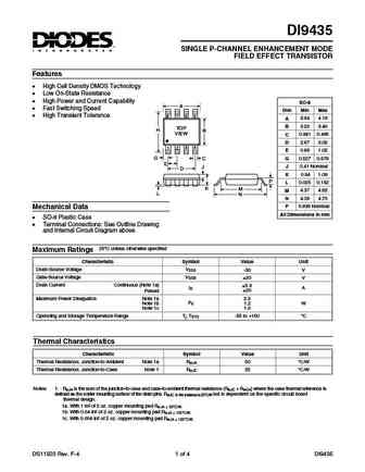
DI9435 SINGLE P-CHANNEL ENHANCEMENT MODE FIELD EFFECT TRANSISTOR Features High Cell Density DMOS Technology Low On-State Resistance High Power and Current Capability SO-8 A Fast Switching Speed Dim Min Max High Transient Tolerance 8 7 6 5 A 3.94 4.19 B 3.20 3.40 TOP H B VIEW C 0.381 0.495 D 2.67 3.05 1 2 3 4 E 0.89 1.02 G C G 0.527 0.679 E J 0.41 Nominal J D K 0.... See More ⇒
fds9435a.pdf
FDS9435A 30V P-Channel PowerTrench Features MOSFET 5.3 A, 30 V R = 50 m @ V = 10 V DS(ON) GS General Description R = 80 m @ V = 4.5 V DS(ON) GS This P-Channel MOSFET is a rugged gate version of ON Low gate charge Semiconductor s advanced PowerTrench process. It has been optimized for power management applications requiring Fast switching speed... See More ⇒
nsv9435t1g.pdf

NSB9435T1G, NSV9435T1G High Current Bias Resistor Transistor PNP Silicon http //onsemi.com Features Collector -Emitter Sustaining Voltage - POWER BJT VCEO(sus) = 30 Vdc (Min) @ IC = 10 mAdc IC = 3.0 AMPERES High DC Current Gain - BVCEO = 30 VOLTS hFE = 125 (Min) @ IC = 0.8 Adc VCE(sat) = 0.275 VOLTS = 90 (Min) @ IC = 3.0 Adc Low Collector -Emitter Saturation Voltag... See More ⇒
nsb9435t1-d.pdf
NSB9435T1G High Current Bias Resistor Transistor PNP Silicon Features http //onsemi.com Collector -Emitter Sustaining Voltage - VCEO(sus) = 30 Vdc (Min) @ IC = 10 mAdc POWER BJT High DC Current Gain - IC = 3.0 AMPERES hFE = 125 (Min) @ IC = 0.8 Adc BVCEO = 30 VOLTS = 90 (Min) @ IC = 3.0 Adc VCE(sat) = 0.275 VOLTS Low Collector -Emitter Saturation Voltage - VCE(sat... See More ⇒
nsb9435t1g nsv9435t1g.pdf

NSB9435T1G, NSV9435T1G High Current Bias Resistor Transistor PNP Silicon http //onsemi.com Features Collector -Emitter Sustaining Voltage - POWER BJT VCEO(sus) = 30 Vdc (Min) @ IC = 10 mAdc IC = 3.0 AMPERES High DC Current Gain - BVCEO = 30 VOLTS hFE = 125 (Min) @ IC = 0.8 Adc VCE(sat) = 0.275 VOLTS = 90 (Min) @ IC = 3.0 Adc Low Collector -Emitter Saturation Voltag... See More ⇒
mmjt9435.pdf
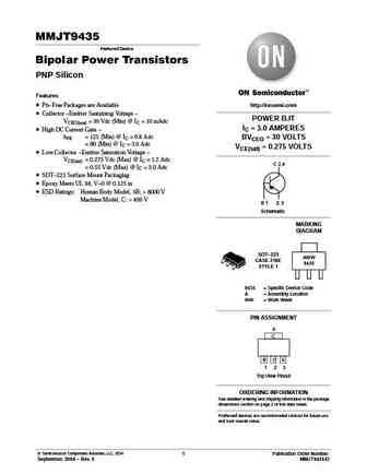
MMJT9435 Preferred Device Bipolar Power Transistors PNP Silicon Features Pb-Free Packages are Available http //onsemi.com Collector -Emitter Sustaining Voltage - POWER BJT VCEO(sus) = 30 Vdc (Min) @ IC = 10 mAdc IC = 3.0 AMPERES High DC Current Gain - hFE = 125 (Min) @ IC = 0.8 Adc BVCEO = 30 VOLTS = 90 (Min) @ IC = 3.0 Adc VCE(sat) = 0.275 VOLTS Low Collector ... See More ⇒
nsb9435t1g.pdf
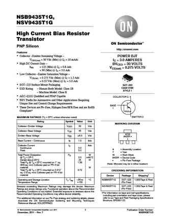
NSB9435T1G, NSV9435T1G High Current Bias Resistor Transistor PNP Silicon http //onsemi.com Features Collector -Emitter Sustaining Voltage - POWER BJT VCEO(sus) = 30 Vdc (Min) @ IC = 10 mAdc IC = 3.0 AMPERES High DC Current Gain - BVCEO = 30 VOLTS hFE = 125 (Min) @ IC = 0.8 Adc VCE(sat) = 0.275 VOLTS = 90 (Min) @ IC = 3.0 Adc Low Collector -Emitter Saturation Voltag... See More ⇒
ut9435hl-aa3-r ut9435hg-aa3-r ut9435hl-ae3-r ut9435hg-ae3-r ut9435hl-al6-r ut9435hg-ag6-r ut9435hl-s08-r ut9435hg-s08-r.pdf
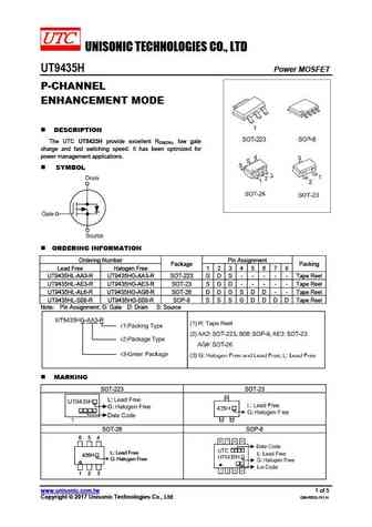
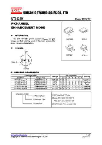
UNISONIC TECHNOLOGIES CO., LTD UT9435H Power MOSFET P-CHANNEL ENHANCEMENT MODE DESCRIPTION The UTC UT9435H provide excellent RDS(ON), low gate charge and fast switching speed. It has been optimized for power management applications. SYMBOL ORDERING INFORMATION Ordering Number Pin Assignment Package Packing Lead Free Halogen Free 1 2 3 4 5 6 7 8 UT9435HL-AA... See More ⇒
ut9435hz.pdf
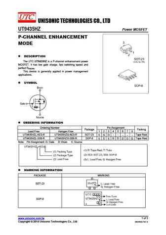
UNISONIC TECHNOLOGIES CO., LTD UT9435HZ Power MOSFET P-CHANNEL ENHANCEMENT MODE DESCRIPTION The UTC UT9435HZ is a P-channel enhancement power MOSFET. It has low gate charge, fast switching speed and perfect RDS(ON). This device is generally applied in power management applications. SYMBOL ORDERING INFORMATION Ordering Number Pin Assignment Package Packing L... See More ⇒
ut9435h.pdf
UNISONIC TECHNOLOGIES CO., LTD UT9435H Power MOSFET P-CHANNEL ENHANCEMENT MODE DESCRIPTION The UTC UT9435H provide excellent RDS(ON), low gate charge and fast switching speed. It has been optimized for power management applications. SYMBOL ORDERING INFORMATION Ordering Number Pin Assignment Package Packing Lead Free Halogen Free 1 2 3 4 5 6 7 8 UT9435HL-AA3-R UT9... See More ⇒
ut9435.pdf
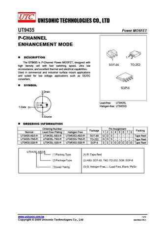
UNISONIC TECHNOLOGIES CO., LTD UT9435 Power MOSFET P-CHANNEL ENHANCEMENT MODE DESCRIPTION The UT9435 is P-Channel Power MOSFET, designed with high density cell with fast switching speed, ultra low on-resistance, and excellent thermal and electrical capabilities. Used in commercial and industrial surface mount applications and suited for low voltage applications such as DC/DC ... See More ⇒
sid9435.pdf
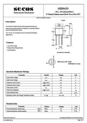
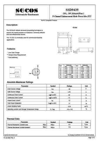
SID9435 -20A, -30V,RDS(ON)50m Elektronische Bauelemente P-Channel Enhancement Mode Power Mos.FET RoHS Compliant Product TO-251 Description 2.3 0.1 6.6 0.2 5.3 0.2 0.5 0.05 The SID9435 utilized advanced processing techniques to achieve the lowest possible on-resistance, extremely efficient and cost-effectiveness device. 7.0 0.2 5.6 0.2 The TO-251 is univ... See More ⇒
ssg9435.pdf
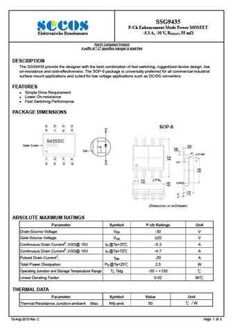
SSG9435 P-Ch Enhancement Mode Power MOSFET -5.3 A, -30 V, RDS(ON) 55 m Elektronische Bauelemente RoHS Compliant Product A suffix of -C specifies halogen & lead-free DESCRIPTION The SSG9435 provide the designer with the best combination of fast switching, ruggedized device design, low on-resistance and cost-effectiveness. The SOP-8 package is universally preferred for all ... See More ⇒
ssd9435.pdf
SSD9435 -20A, -30V,RDS(ON)50m Elektronische Bauelemente P-Channel Enhancement Mode Power Mos.FET RoHS Compliant Product Description TO-252 The SSD9435 utilized advanced processing techniques to achieve the lowest possible on-resistance, extremely efficient and cost-effectiveness device. The TO-252 is universally used for commercial-industrial applications. Features * Lo... See More ⇒
ssg9435bdy.pdf
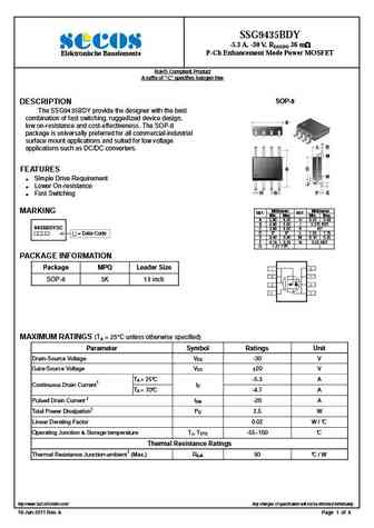
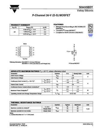
SSG9435BDY -5.3 A, -30 V, RDS(ON) 36 m P-Ch Enhancement Mode Power MOSFET Elektronische Bauelemente RoHS Compliant Product A suffix of -C specifies halogen free SOP-8 DESCRIPTION The SSG9435BDY provide the designer with the best combination of fast switching, ruggedized device design, B low on-resistance and cost-effectiveness. The SOP-8 package is... See More ⇒
ssg9435p.pdf
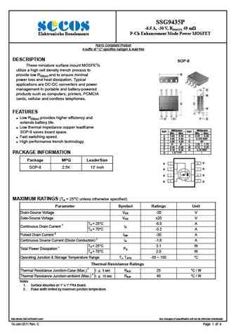
SSG9435P -6.5 A, -30 V, RDS(ON) 49 m P-Ch Enhancement Mode Power MOSFET Elektronische Bauelemente RoHS Compliant Product A suffix of -C specifies halogen & lead-free DESCRIPTION SOP-8 These miniature surface mount MOSFETs utilize a high cell density trench process to B provide low RDS(on) and to ensure minimal power loss and heat dissipation. Typical applicat... See More ⇒
tsm9435cs.pdf
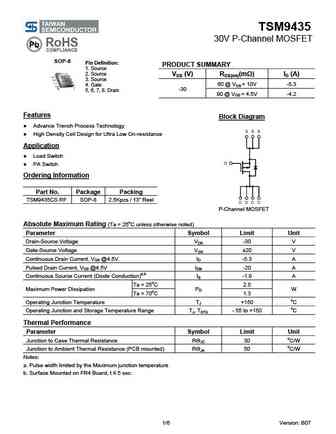
TSM9435 30V P-Channel MOSFET SOP-8 Pin Definition PRODUCT SUMMARY 1. Source 2. Source VDS (V) RDS(on)(m ) ID (A) 3. Source 60 @ VGS = 10V -5.3 4. Gate -30 5, 6, 7, 8. Drain 90 @ VGS = 4.5V -4.2 Features Block Diagram Advance Trench Process Technology High Density Cell Design for Ultra Low On-resistance Application Load Switch PA Swit... See More ⇒
cjq9435.pdf
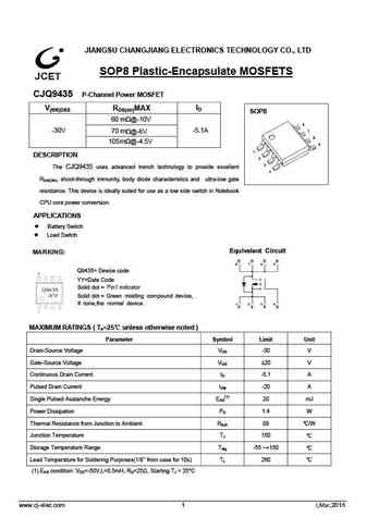
JIANGSU CHANGJIANG ELECTRONICS TECHNOLOGY CO., LTD SOP8 Plastic-Encapsulate MOSFETS CJQ9435 P-Channel Power MOSFET I D V (BR)DSS R DS(on) MAX SOP8 60 m @-10V -30V -5.1A m 70 @-6V 105m @-4.5V DESCRIPTION The CJQ9435 uses advanced trench technology to provide excellent RDS(ON), shoot-through immunity, body diode characteristics and ultra-low gate resistance. This de... See More ⇒
cet9435a.pdf
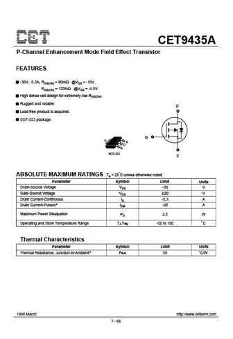
CET9435A P-Channel Enhancement Mode Field Effect Transistor FEATURES -30V, -5.3A, RDS(ON) = 60m @VGS = -10V. RDS(ON) = 120m @VGS = -4.5V. High dense cell design for extremely low RDS(ON). Rugged and reliable. D Lead free product is acquired. SOT-223 package. G D S D G SOT-223 S ABSOLUTE MAXIMUM RATINGS TA = 25 C unless otherwise noted Parameter Symbol Limit Units Drain... See More ⇒
cem9435.pdf
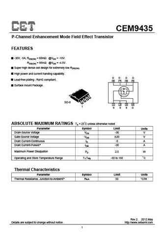
CEM9435 P-Channel Enhancement Mode Field Effect Transistor FEATURES -30V, -5A, RDS(ON) = 60m @VGS = -10V. RDS(ON) = 95m @VGS = -4.5V. Super high dense cell design for extremely low RDS(ON). High power and current handing capability. D D D D Lead-free plating ; RoHS compliant. 8 7 6 5 Surface mount Package. SO-8 1 2 3 4 1 S S S G ABSOLUTE MAXIMUM RATINGS TA = 25 C unless o... See More ⇒
wtk9435.pdf
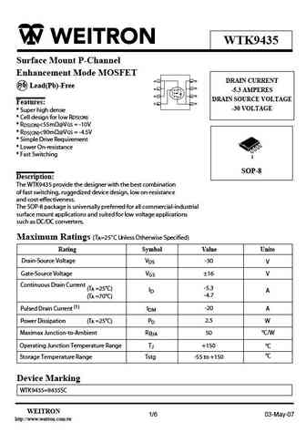
WTK9435 Surface Mount P-Channel Enhancement Mode MOSFET DRAIN CURRENT P b Lead(Pb)-Free -5.3 AMPERES DRAIN SOURCE VOLTAGE Features -30 VOLTAGE * Super high dense * Cell design for low RDS(ON) * R ... See More ⇒
wtc9435.pdf
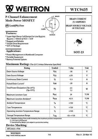
WTC9435 3 DRAIN P-Channel Enhancement DRAIN CURRENT Mode Power MOSFET -5.3 AMPERES P b Lead(Pb)-Free 1 DRAIN SOURCE VOLTAGE -30 VOLTAGE GATE 2 Features SOURCE * Super High Dense Cell Design For Low RDS(on) RDS(on) ... See More ⇒
wtd9435.pdf
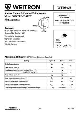
WTD9435 Surface Mount P-Channel Enhancement DRAIN CURRENT Mode POWER MOSFET 3 DRAIN -20 AMPERES P b Lead(Pb)-Free DRAIN SOURCE VOLTAGE -30 VOLTAGE 1 GATE Features 2 *Super High Dense Cell Design For Low RDS(ON) SOURCE RDS(ON)... See More ⇒
wtn9435.pdf
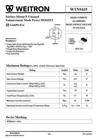
WTN9435 Surface Mount P-Channel DRAIN CURRENT Enhancement Mode Power MOSFET -6.0 AMPERES 2,4 DRAIN DRAIN SOURCE VOLTAGE P b Lead(Pb)-Free -30 VOLTAGE 1 GATE 4 1. GATE 2. DRAIN Features 1 3. SOURCE 3 2 SOURCE 4. DRAIN 3 * Super high dense cell design for low RDS(ON) RDS(ON) ... See More ⇒
se9435lt1.pdf
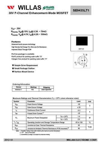
FM120-M WILLAS THRU SE9435LT1 30V P-Channel Enhancement-Mode MOSFET FM1200-M 1.0A SURFACE MOUNT SCHOTTKY BARRIER RECTIFIERS -20V- 200V SOD-123 PACKAGE Pb Free Product Package outline Features Batch process design, excellent power dissipation offers better reverse leakage current and thermal resistance. SOD-123H Low profile surface mounted application in order to ... See More ⇒
wpm9435.pdf
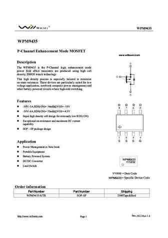
WPM9435 WPM9435 P-Channel Enhancement Mode MOSFET www.willsemi.com Description The WPM9435 is the P-Channel logic enhancement mode power field effect transistors are produced using high cell density, DMOS trench technology. This high density process is especially tailored to minimize on-state resistance. These devices are particularly suited for low voltage application, noteb... See More ⇒
h9435s.pdf
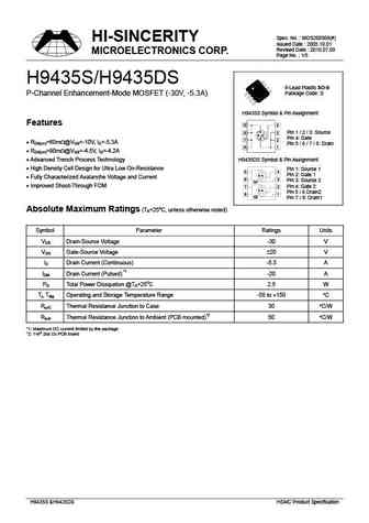
Spec. No. MOS200509(#) HI-SINCERITY Issued Date 2005.10.01 Revised Date 2010.07.08 MICROELECTRONICS CORP. Page No. 1/5 H9435S/H9435DS 8-Lead Plastic SO-8 Package Code S P-Channel Enhancement-Mode MOSFET (-30V, -5.3A) H9435S Symbol & Pin Assignment Features 5 4 6 3 Pin 1 / 2 / 3 Source Pin 4 Gate 7 2 RDS(on)=60m @VGS=-10V, ID=-5.3A Pin 5 / 6 ... See More ⇒
ap9435gm-hf.pdf
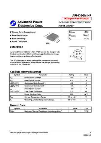
AP9435GM-HF Halogen-Free Product Advanced Power P-CHANNEL ENHANCEMENT MODE Electronics Corp. POWER MOSFET Simple Drive Requirement BVDSS -30V D D D Low Gate Charge RDS(ON) 50m D Fast Switching ID -5.3A G S RoHS Compliant S S SO-8 Description D Advanced Power MOSFETs from APEC provide the designer with the best combination of fast switching, ruggedized devic... See More ⇒
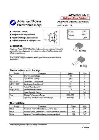
ap9435gh ap9435gj.pdf
AP9435GH/J RoHS-compliant Product Advanced Power P-CHANNEL ENHANCEMENT MODE Electronics Corp. POWER MOSFET Low Gate Charge BVDSS -30V D Simple Drive Requirement RDS(ON) 50m Fast Switching ID - 20A G S Description G D Advanced Power MOSFETs utilized advanced processing techniques to S TO-252(H) achieve the lowest possible on-resistance, extremely efficient and cost- ... See More ⇒
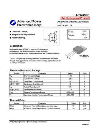
ap9435gp-hf.pdf
AP9435GP-HF Halogen-Free Product Advanced Power P-CHANNEL ENHANCEMENT MODE Electronics Corp. POWER MOSFET Low Gate Charge BVDSS -30V D Simple Drive Requirement RDS(ON) 50m Fast Switching Characteristic ID - 15A G RoHS Compliant & Halogen-Free S Description Advanced Power MOSFETs from APEC provide the designer with the best combination of fast switching, ruggedized... See More ⇒
ap9435gm.pdf
AP9435GM RoHS-compliant Product Advanced Power P-CHANNEL ENHANCEMENT MODE Electronics Corp. POWER MOSFET Simple Drive Requirement BVDSS -30V D D D Low Gate Charge RDS(ON) 50m D Fast Switching ID -5.3A G S S S SO-8 Description D The Advanced Power MOSFETs from APEC provide the designer with the best combination of fast switching, ruggedized device design, low on... See More ⇒
ap9435gk-hf.pdf
AP9435GK-HF Halogen-Free Product Advanced Power P-CHANNEL ENHANCEMENT MODE Electronics Corp. POWER MOSFET Simple Drive Requirement BVDSS -30V D Low Gate Charge RDS(ON) 50m Fast Switching Characteristic ID -6A S D RoHS Compliant & Halogen-Free SOT-223 G Description D Advanced Power MOSFETs from APEC provide the designer with the best combination of fast switchi... See More ⇒
ap9435gp.pdf
AP9435GP RoHS-compliant Product Advanced Power P-CHANNEL ENHANCEMENT MODE Electronics Corp. POWER MOSFET Low Gate Charge BVDSS -30V D Simple Drive Requirement RDS(ON) 50m Fast Switching ID - 15A G S Description Advanced Power MOSFETs from APEC provide the designer with the best combination of fast switching, ruggedized device design, low on-resistance and cost-effecti... See More ⇒
ap9435gj-hf.pdf
AP9435GH/J-HF Halogen-Free Product Advanced Power P-CHANNEL ENHANCEMENT MODE Electronics Corp. POWER MOSFET Low Gate Charge BVDSS -30V D Simple Drive Requirement RDS(ON) 50m Fast Switching Characteristic ID - 20A G RoHS Compliant & Halogen-Free S Description Advanced Power MOSFETs utilized advanced processing techniques to G D S TO-252(H) achieve the lowest poss... See More ⇒
ap9435gg-hf.pdf
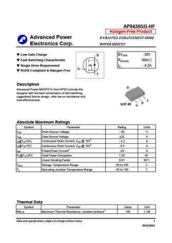
AP9435GG-HF Halogen-Free Product Advanced Power P-CHANNEL ENHANCEMENT MODE Electronics Corp. POWER MOSFET Low Gate Charge BVDSS -30V D Fast Switching Characteristic RDS(ON) 50m Single Drive Requirement ID - 4.2A G RoHS Compliant & Halogen-Free S Description D Advanced Power MOSFETs from APEC provide the designer with the best combination of fast switching, rugge... See More ⇒
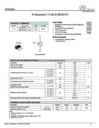
am9435p.pdf
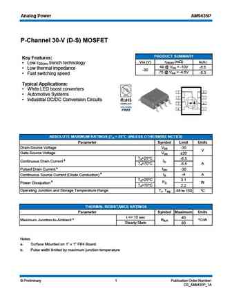
Analog Power AM9435P P-Channel 30-V (D-S) MOSFET PRODUCT SUMMARY Key Features rDS(on) (m ) VDS (V) ID(A) Low r trench technology DS(on) 49 @ VGS = -10V -6.5 Low thermal impedance -30 75 @ VGS = -4.5V -5.3 Fast switching speed Typical Applications White LED boost converters Automotive Systems Industrial DC/DC Conversion Circuits ABSOLUTE MAXIMU... See More ⇒
afp9435ws.pdf
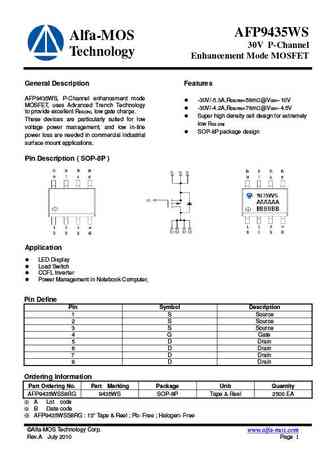
AFP9435WS Alfa-MOS 30V P-Channel Technology Enhancement Mode MOSFET General Description Features AFP9435WS, P-Channel enhancement mode -30V/-5.3A,RDS(ON)=58m @VGS=-10V MOSFET, uses Advanced Trench Technology -30V/-4.2A,RDS(ON)=78m @VGS=-4.5V to provide excellent RDS(ON), low gate charge. Super high density cell design for extremely These devices are particularly s... See More ⇒
afp9435s.pdf
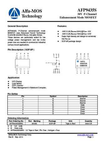
AFP9435S Alfa-MOS 30V P-Channel Technology Enhancement Mode MOSFET General Description Features AFP9435S, P-Channel enhancement mode -30V/-5.3A,RDS(ON)=52m @VGS=-10V MOSFET, uses Advanced Trench Technology -30V/-4.2A,RDS(ON)=76m @VGS=-4.5V to provide excellent RDS(ON), low gate charge. Super high density cell design for extremely These devices are particularly sui... See More ⇒
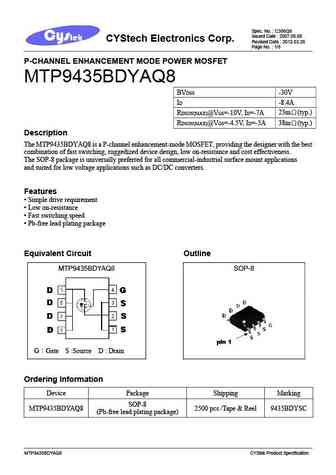
mtp9435bdyq8.pdf
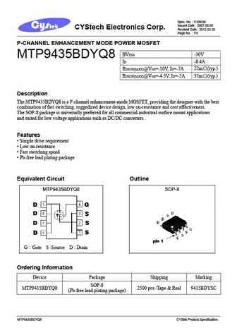
Spec. No. C386Q8 Issued Date 2007.06.08 CYStech Electronics Corp. Revised Date 2012.03.26 Page No. 1/8 P-CHANNEL ENHANCEMENT MODE POWER MOSFET BVDSS -30V MTP9435BDYQ8 ID -8.4A 22m (typ.) RDSON(MAX)@VGS=-10V, ID=-7A 35m (typ.) RDSON(MAX)@VGS=-4.5V, ID=-5A Description The MTP9435BDYQ8 is a P-channel enhancement-mode MOSFET, providing the designer with the best ... See More ⇒
btb9435j3.pdf
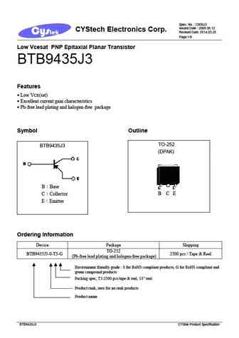
Spec. No. C809J3 Issued Date 2008.06.12 CYStech Electronics Corp. Revised Date 2014.03.25 Page 1/8 Low Vcesat PNP Epitaxial Planar Transistor BTB9435J3 Features Low VCE(sat) Excellent current gain characteristics Pb-free lead plating and halogen-free package Symbol Outline TO-252 BTB9435J3 (DPAK) B Base B C E C Collector E Emitter O... See More ⇒
mtp9435l3.pdf
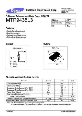
Spec. No. C400L3 Issued Date 2009.06.22 CYStech Electronics Corp. Revised Date Page No. 1/7 P-Channel Enhancement Mode Power MOSFET BVDSS -30V MTP9435L3 RDSON(MAX) 60m ID -6A Features Simple Drive Requirement Low On-resistance Fast switching Characteristic Pb-free lead plating package Symbol Outline SOT-223 MTP9435L3 D S G Gate ... See More ⇒
mtp9435q8.pdf
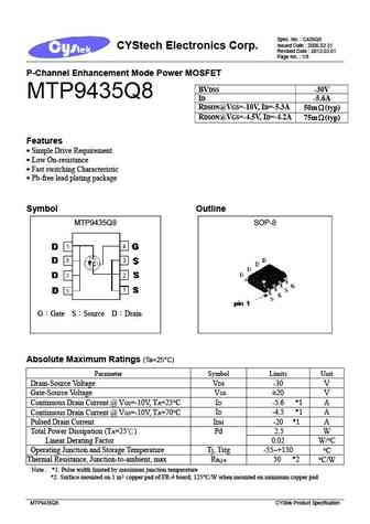
Spec. No. C426Q8 Issued Date 2006.03.31 CYStech Electronics Corp. Revised Date 2013.03.01 Page No. 1/8 P-Channel Enhancement Mode Power MOSFET BVDSS -30V MTP9435Q8 ID -5.6A RDSON@VGS=-10V, ID=-5.3A 50m (typ) RDSON@VGS=-4.5V, ID=-4.2A 75m (typ) Features Simple Drive Requirement Low On-resistance Fast switching Characteristic Pb-free lead plat... See More ⇒
mtp9435bdyaq8.pdf
Spec. No. C386Q8 Issued Date 2007.06.08 CYStech Electronics Corp. Revised Date 2012.03.26 Page No. 1/8 P-CHANNEL ENHANCEMENT MODE POWER MOSFET MTP9435BDYAQ8 BVDSS -30V ID -8.4A 23m (typ.) RDSON(MAX)@VGS=-10V, ID=-7A 38m (typ.) RDSON(MAX)@VGS=-4.5V, ID=-5A Description The MTP9435BDYAQ8 is a P-channel enhancement-mode MOSFET, providing the designer with the best ... See More ⇒
btb9435l3.pdf
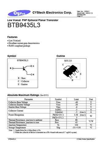
Spec. No. C809L3 CYStech Electronics Corp. Issued Date 2009.01.16 Revised Date Page 1/7 Low Vcesat PNP Epitaxial Planar Transistor BTB9435L3 Features Low VCE(sat) Excellent current gain characteristics RoHS compliant package Symbol Outline BTB9435L3 SOT-223 C E C B Base B C Collector E Emitter Absolute Maximum Ratings (Ta=25 C) P... See More ⇒
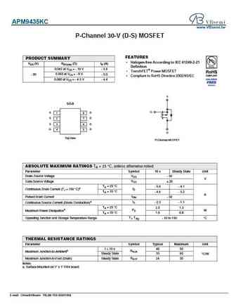
apm9435.pdf
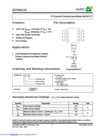
APM9435 P-Channel Enhancement Mode MOSFET Features Pin Description -30V/-4.6A, RDS(ON) = 52m (typ.) @ VGS = -10V S 1 8 D RDS(ON) = 80m (typ.) @ VGS = -4.5V S 2 7 D Super High Density Cell Design S 3 6 D Reliable and Rugged G 45 D SO-8 Package SO - 8 Applications S S S Power Management in Noteboo... See More ⇒
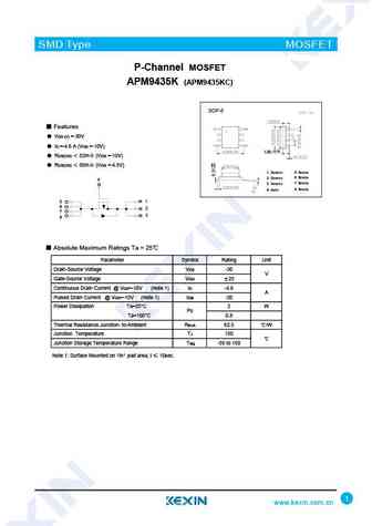
apm9435k.pdf
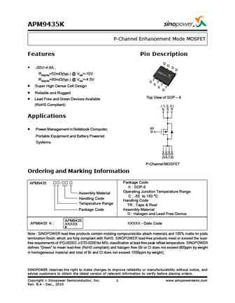
APM9435K P-Channel Enhancement Mode MOSFET Features Pin Description D D -30V/-4.6A , D D RDS(ON)=52m (typ.) @ VGS=-10V RDS(ON)=80m (typ.) @ VGS=-4.5V S S Super High Dense Cell Design S G Reliable and Rugged Top View of SOP - 8 Lead Free and Green Devices Available (RoHS Compliant) ( 1, 2, 3 ) S S S Applications (4) Power Management in Notebook Computer, ... See More ⇒
stm9435.pdf
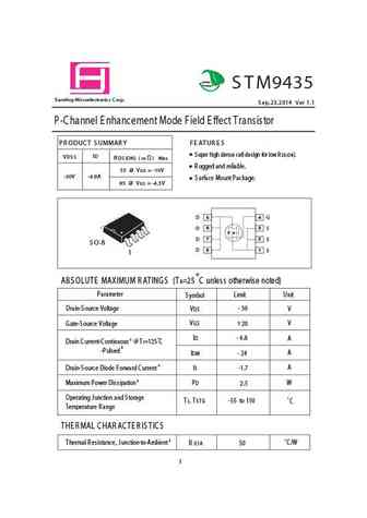
Green Product S T M9435 S amHop Microelectronics C orp. S ep,23,2014 Ver 1.1 P-C hannel E nhancement Mode Field E ffect Transistor P R ODUC T S UMMAR Y FEATURES S uper high dense cell design for low R DS (ON). V DS S ID R DS (ON) ( m ) Max R ugged and reliable. 55 @ V GS = -10V -30V -4.8A S urface Mount Package. 85 @ V GS = -4.5V D 5 4 G 6 3 D S 7 2 D S SO-8 D 8 1 S 1... See More ⇒
ssf9435.pdf
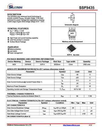
SSF9435 D DESCRIPTION The SSF9435 uses advanced trench technology to G provide excellent RDS(ON), low gate charge .It has been optimized for power management applications requiring a wide range of gave drive voltage ratings (4.5V 25V). S Schematic diagram D D D D GENERAL FEATURES 7 6 5 8 VDS = -30V,ID = -5.3A RDS(ON) ... See More ⇒
brcs9435sc.pdf
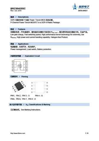
BRCS9435SC Rev. I Jan.-2019 DATA SHEET / Descriptions SOP-8 P Power Trench MOS P-Channel Power Trench MOSFET in a SOP-8 Plastic Package. / Features RDS ON Low gate charge, Fast switching speed, High ... See More ⇒
st2sb9435u.pdf
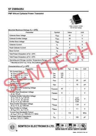
ST 2SB9435U PNP Silicon Epitaxial Power Transistor Absolute Maximum Ratings (Ta = 25 ) Parameter Symbol Value Unit Collector Base Voltage -VCBO 45 V Collector Emitter Voltage -VCEO 30 V Emitter Base Voltage -VEBO 6 V Collector Current -IC 3 A Peak Collector Current -ICM 5 A Base Current -IB 1 A 1) Total Power Dissipation at Ta = 25 Ptot 0.72 W Total Power Dissipation at Tc =... See More ⇒
lp9435lt1g.pdf
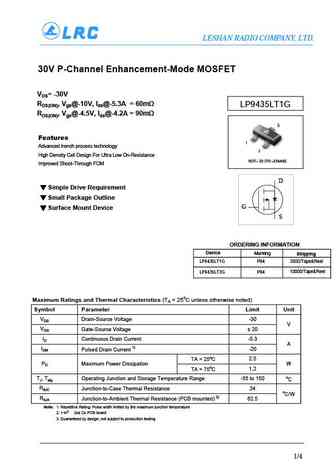
LESHAN RADIO COMPANY, LTD. 30V P-Channel Enhancement-Mode MOSFET VDS= -30V RDS(ON), Vgs@-10V, Ids@-5.3A = 60m LP9435LT1G RDS(ON), Vgs@-4.5V, Ids@-4.2A = 90m 3 Features 1 Advanced trench process technology 2 High Density Cell Design For Ultra Low On-Resistance SOT 23 (TO 236AB) Improved Shoot-Through FOM D Simple Drive Requirement Small Pack... See More ⇒
sm9435psk.pdf
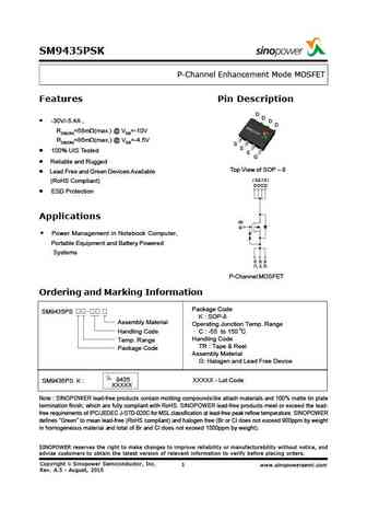
SM9435PSK P-Channel Enhancement Mode MOSFET Features Pin Description D D -30V/-5.4A , D D RDS(ON)=58m (max.) @ VGS=-10V RDS(ON)=86m (max.) @ VGS=-4.5V S S 100% UIS Tested S G Reliable and Rugged Top View of SOP - 8 Lead Free and Green Devices Available ( 5,6,7,8 ) (RoHS Compliant) DDDD ESD Protection Applications (4) G Power Management in Notebook Comp... See More ⇒
ftk9435.pdf
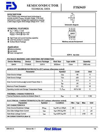
SEMICONDUCTOR FTK9435 TECHNICAL DATA D DESCRIPTION The FTK9435 uses advanced trench technology to G provide excellent RDS(ON), low gate charge .It has been optimized for power management applications requiring a wide range of gave drive voltage ratings (4.5V 25V). S Schematic diagram D D D D GENERAL FEATURES 7 6 5 8 VDS = -30V,ID = -5.3A RDS(ON) ... See More ⇒
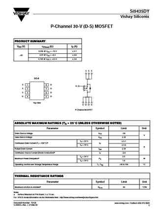
si9435dy.pdf

SMD Type MOSFET P-Channel MOSFET SI9435DY SOP-8 Features VDS (V) =-30V ID =-5.3 A (VGS =-10V) 1.50 0.15 RDS(ON) 50m (VGS =-10V) RDS(ON) 80m (VGS =-4.5V) Fast switching speed 1 Source 5 Drain 6 Drain 2 Source 7 Drain 3 Source 8 Drain 4 Gate 5 4 6 3 7 2 8 1 Absolute Maximum Ratings Ta = 25 Parameter Symbol Rating Unit Drain-... See More ⇒
apm9435k.pdf
SMD Type MOSFET P-Channel MOSFET APM9435K (APM9435KC) SOP-8 Features VDS (V) =-30V ID =-4.6 A (VGS =-10V) 1.50 0.15 RDS(ON) 52m (VGS =-10V) RDS(ON) 80m (VGS =-4.5V) 1 Source 5 Drain 6 Drain 2 Source 4 7 Drain 3 Source G 8 Drain 4 Gate 5 1 6 2 7 3 8 Absolute Maximum Ratings Ta = 25 Parameter Symbol Rating Unit Drain-Source Vo... See More ⇒
kx9435.pdf
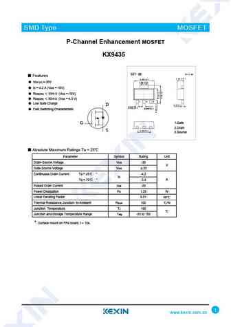
SMD Type MOSFET P-Channel Enhancement MOSFET KX9435 Features VDS (V) =-30V 1.70 0.1 ID =-4.2 A (VGS =-10V) RDS(ON) 55m (VGS =-10V) RDS(ON) 90m (VGS =-4.5 V) Low Gate Charge D 0.42 0.1 0.46 0.1 Fast Switching Characteristic 1.Gate G 2.Drain S 3.Source Absolute Maximum Ratings Ta = 25 Parameter Symbol Rating Unit Drain-Sou... See More ⇒
ki9435dy.pdf
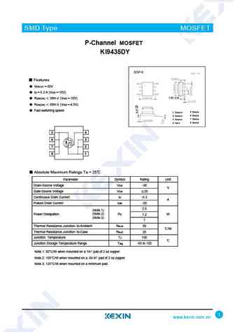
SMD Type MOSFET P-Channel MOSFET KI9435DY SOP-8 Features VDS (V) =-30V ID =-5.3 A (VGS =-10V) 1.50 0.15 RDS(ON) 58m (VGS =-10V) RDS(ON) 89m (VGS =-4.5V) Fast switching speed 1 Source 5 Drain 6 Drain 2 Source 7 Drain 3 Source 8 Drain 4 Gate 5 4 6 3 7 2 8 1 Absolute Maximum Ratings Ta = 25 Parameter Symbol Rating Unit Drain... See More ⇒
si9435bdy.pdf
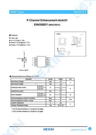
SMD Type IC SMD Type MOSFET P-Channel Enhancement MOSFET SI9435BDY (KI9435BDY) SOP-8 Features VDSS = -30V ID = -5.7A (VGS = -10V) RDS(ON) = 42 m @ VGS = -10 V 1.50 0.15 RDS(ON) = 70 m @ VGS = -4.5 V S S D 1 8 G S D 2 7 S D 3 6 G D 4 5 D P-Channel MOSFET Absolute Maximum Ratings Ta = 25 Parameter Symbol Rating Unit Drain-Source Voltag... See More ⇒
am9435.pdf
AM9435 AiT Semiconductor Inc. www.ait-ic.com MOSFET -30V P-CHANNEL ENHANCEMENT MODE DESCRIPTION FEATURES The AM9435 is the P-Channel logic enhancement -30V/-5.8A, R =38m (typ.)@V =-10V DS(ON) GS mode power field effect transistor is produced using -30V/-4.0A, R =60m (typ.)@V =-4.5V DS(ON) GS high cell density, advanced trench technology to Super high density cell desig... See More ⇒
am9435.pdf
AM9435 -30V P-Channel Enhancement Mode MOSFET DESCRIPTION FEATURE The AM9435 is the P-Channel logic enhancement -30V/-5.2A, RDS(ON) 60m @VGS = -10V mode power field effect transistors are produced -30V/-4.0A, RDS(ON) 90m @VGS = -4.5V using high cell density, DMOS trench technology. Super high density cell design for extremely low This high density process... See More ⇒
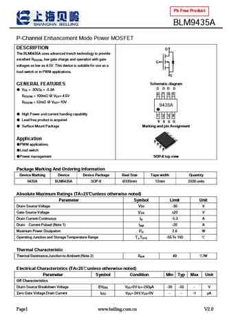
blm9435.pdf
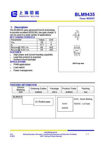
BLM9435 Power MOSFET 1 Description Step-Down Converter The BLM9435 uses advanced trench technology , to provide excellent RDS(ON), low gate charge. It can be used in a wide variety of applications. KEY CHARACTERISTICS Parameter Value Unit V -30 V DS I -5.1 A D R .TYP 48 m DS(ON)@-10V R .TYP 70 m DS(ON)@-4.5V FEATURES High power and current handi... See More ⇒
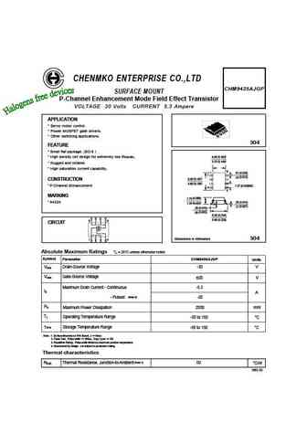
chm9435azgp.pdf
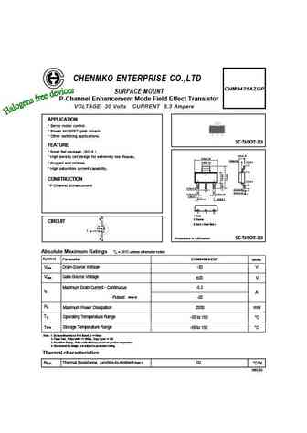
CHENMKO ENTERPRISE CO.,LTD CHM9435AZGP SURFACE MOUNT P-Channel Enhancement Mode Field Effect Transistor VOLTAGE 30 Volts CURRENT 5.3 Ampere APPLICATION * Servo motor control. * Power MOSFET gate drivers. * Other switching applications. SC-73/SOT-223 FEATURE * Small flat package. (SO-8 ) 1.65+0.15 * High density cell design for extremely low RDS(ON). 6.50+0.20 0.90+0.05 2.0+0... See More ⇒
chm9435gp.pdf
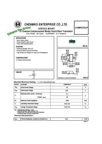
CHENMKO ENTERPRISE CO.,LTD CHM9435GP SURFACE MOUNT P-Channel Enhancement Mode Field Effect Transistor VOLTAGE 30 Volts CURRENT 5.3 Ampere APPLICATION * Servo motor control. * Power MOSFET gate drivers. * Other switching applications. SOT-23 FEATURE * Small flat package. (SOT-23) * Advanced trench process technology * High Density Cell Design For Ultra Low On-Resistance (1) (... See More ⇒
cht9435zgp.pdf
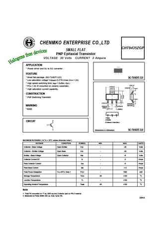
CHENMKO ENTERPRISE CO.,LTD CHT9435ZGP SMALL FLAT PNP Epitaxial Transistor VOLTAGE 30 Volts CURRENT 3 Ampere APPLICATION * Power driver and Dc to DC convertor . FEATURE * Small flat package. (SC-73/SOT-223) SC-73/SOT-223 * Low saturation voltage VCE(sat)=-0.275V(max.)(IC=-1.2A) * High speed switching time tstg= 1.0uSec (typ.) 1.65+0.15 * PC= 1.56 W (mounted on ceramic substrate)... See More ⇒
chm9435ajgp.pdf
CHENMKO ENTERPRISE CO.,LTD CHM9435AJGP SURFACE MOUNT P-Channel Enhancement Mode Field Effect Transistor VOLTAGE 30 Volts CURRENT 5.3 Ampere APPLICATION * Servo motor control. * Power MOSFET gate drivers. * Other switching applications. SO-8 FEATURE * Small flat package. (SO-8 ) ( ) * High density cell design for extremely low RDS(ON). 4.06 0.160 ( ) 3.70 0.146 * Rugged and re... See More ⇒
gsm9435s.pdf
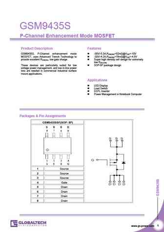
GSM9435S P-Channel Enhancement Mode MOSFET Product Description Features GSM9435S, P-Channel enhancement mode -30V/-5.3A,RDS(ON)=52m @VGS=-10V MOSFET, uses Advanced Trench Technology to -30V/-4.2A,RDS(ON)=76m @VGS=-4.5V provide excellent RDS(ON), low gate charge. Super high density cell design for extremely low RDS (ON) These devices are particularly suited for low... See More ⇒
gsm9435ws.pdf
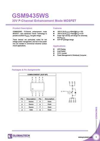
GSM9435WS 30V P-Channel Enhancement Mode MOSFET Product Description Features GSM9435WS, P-Channel enhancement mode -30V/-5.3A,RDS(ON)=58m @VGS=-10V MOSFET, uses Advanced Trench Technology to -30V/-4.2A,RDS(ON)=78m @VGS=-4.5V provide excellent RDS(ON), low gate charge. Super high density cell design for extremely low RDS (ON) These devices are particularly suited f... See More ⇒
me9435as me9435as-g.pdf
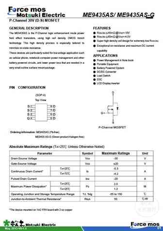
ME9435AS/ ME9435AS-G P-Channel 30V (D-S) MOSFET GENERAL DESCRIPTION FEATURES RDS(ON) 45m @VGS=-10V The ME9435AS is the P-Channel logic enhancement mode power RDS(ON) 60m @VGS=-4.5V field effect transistors, using high cell density, DMOS trench Super high density cell design for extremely low RDS(ON) technology. This high density process is especially tailored t... See More ⇒
me9435a me9435a-g.pdf
ME9435A/ME9435A-G P-Channel 30V (D-S) MOSFET GENERAL DESCRIPTION FEATURES RDS(ON) 40m @VGS=-10V The ME9435A is the P-Channel logic enhancement mode power field RDS(ON) 60m @VGS=-4.5V effect transistors, using high cell density, DMOS trench technology. Super high density cell design for extremely low RDS(ON) This high density process is especially tailored to m... See More ⇒
me9435 me9435-g.pdf
ME9435/ ME9435-G P-Channel 30V (D-S) MOSFET GENERAL DESCRIPTION FEATURES RDS(ON) 60m @VGS=-10V The ME9435 is the P-Channel logic enhancement mode power field RDS(ON) 90m @VGS=-4.5V effect transistors, using high cell density, DMOS trench technology. Super high density cell design for extremely low RDS(ON) This high density process is especially tailored to mini... See More ⇒
mmp9435bdy.pdf
MMP9435BDY Data Sheet M-MOS Semiconductor Hong Kong Limited 30V P- Channel Enhancement-Mode MOSFET VDS= -30V RDS(ON), Vgs@-10V, Ids@-5.7A = 42m RDS(ON), Vgs@-4.5V, Ids@-4.4A = 70m Features Advanced trench process technology High Density Cell Design For Ultra Low On-Resistance Improved Shoot-Through FOM SOP-08 Internal Schematic Diagram Top View P-Channel MOSFET Maximum Rating... See More ⇒
mmp9435.pdf
MMP9435 Data Sheet M-MOS Semiconductor Hong Kong Limited 30V P-Channel Enhancement-Mode MOSFET VDS= -30V RDS(ON), Vgs@-10V, Ids@-5.3A = 60m RDS(ON), Vgs@-4.5V, Ids@-4.2A = 90m Features Advanced trench process technology High Density Cell Design For Ultra Low On-Resistance Improved Shoot-Through FOM SOP-08 Internal Schematic Diagram Top View P-Channel MOSFET Maximum Ratings an... See More ⇒
nce9435a.pdf
http //www.ncepower.com NCE9435A NCE P-Channel Enhancement Mode Power MOSFET Description D The NCE9435A uses advanced trench technology to provide excellent RDS(ON), low gate charge and operation with gate G voltages as low as 4.5V. This device is suitable for use as a load switch or in PWM applications. S Schematic diagram General Features VDS = -30V,ID = -5.3A RDS(... See More ⇒
nce9435.pdf
Pb Free Product http //www.ncepower.com NCE9435 NCE P-Channel Enhancement Mode Power MOSFET D Description The NCE9435 uses advanced trench technology to provide G excellent RDS(ON), low gate charge and operation with gate voltages as low as 4.5V. This device is suitable for use as a load switch or in PWM applications. S Schematic diagram General Features VDS = -30V,ID... See More ⇒
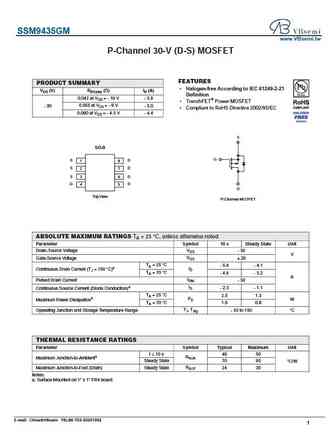
ssm9435gm.pdf
SSM9435GM P-channel Enhancement-mode Power MOSFET PRODUCT SUMMARY DESCRIPTION The SSM9435GM acheives fast switching performance BVDSS -30V with low gate charge without a complex drive circuit. It RDS(ON) 50m is suitable for low voltage applications such as battery management and general high-side switch circuits. I -5.3A D The SSM9435GM is supplied in an RoHS-compliant Pb-free; ... See More ⇒
ssm9435k.pdf
SSM9435K P-CHANNEL ENHANCEMENT-MODE POWER MOSFET Simple drive requirement BV -30V DSS D Low on-resistance R 50m DS(ON) S Fast switching ID -6A D G SOT-223 Description D Advanced Power MOSFETs from Silicon Standard provide the designer with the best combination of fast switching, G low on-resistance and cost-effectiveness. S Absolute Maximum Ratings Symbol Parameter Ratin... See More ⇒
ssm9435gh ssm9435gj.pdf
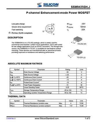
SSM9435GH,J P-channel Enhancement-mode Power MOSFET Low gate-charge BVDSS -30V D Simple drive requirement R 50m DS(ON) Fast switching ID -20A G Pb-free; RoHS compliant. S DESCRIPTION G The SSM9435H is in a TO-252 package, which is widely used for D S TO-252 (H) commercial and industrial surface mount applications, and is well suited for low voltage applications such as DC/DC ... See More ⇒
sl9435a.pdf
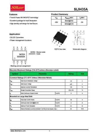
SL9435A Product Summary Features Trench Power MV MOSFET technology VDS RDS(ON) MAX ID MAX Excellent package for heat dissipation 60m @10VD2 S1 -30V -5A D1 High density cell design for low RDS(ON) 90m @4.5V D D D D Application DC-DC Converters Power management functions S S S G D D D D SOP-8 top view Schematic diagram 9435A Device code XXXXXX C... See More ⇒
stp9435.pdf
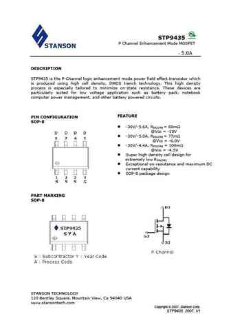
STP9435 P Channel Enhancement Mode MOSFET - 5.0A DESCRIPTION STP9435 is the P-Channel logic enhancement mode power field effect transistor which is produced using high cell density, DMOS trench technology. This high density process is especially tailored to minimize on-state resistance. These devices are particularly suited for low voltage application such as battery pack, note... See More ⇒
st9435a.pdf
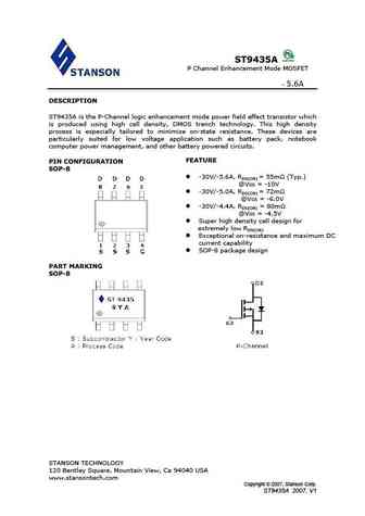
ST9435A P Channel Enhancement Mode MOSFET - 5.6A DESCRIPTION ST9435A is the P-Channel logic enhancement mode power field effect transistor which is produced using high cell density, DMOS trench technology. This high density process is especially tailored to minimize on-state resistance. These devices are particularly suited for low voltage application such as battery pack, note... See More ⇒
st9435gp.pdf
ST9435GP P Channel Enhancement Mode MOSFET -15.0A DESCRIPTION ST9435GP is the P-Channel logic enhancement mode power field effect transistor which is produced using high cell density, DMOS trench technology. This high density process is especially tailored to minimize on-state resistance. These device is particularly suited for low voltage application, notebook computer power... See More ⇒
atm9435ppa.pdf
ATM9435PPA P-Channel Enhancement Mode Field Effect Transistor Description SOP-8L D The ATM9435PPA uses advanced trench technology to provide excellent R , low gate charge and DS(ON) operation with gate voltages as low as -4.5V. This G device is suitable for use as a load switch or in PWM applications. Standard Product ATM9435PPA is Pb- Pin 1 free. S Top View Schematic Feature ... See More ⇒
es9435.pdf
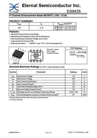
Eternal Semiconductor Inc. ES9435 P-Channel Enhancement-Mode MOSFET (-30V, -5.3A) PRODUCT SUMMARY VDSS ID RDS(on) (m )TYP 50 @ VGS = -10 V, ID=-5.3A -30V -5.3A 70 @ VGS = -4.5V, ID=-4.2A Features Advanced Trench Process Technology High Density Cell Design for Ultra Low On-Resistance Fully Characterized Avalanche Voltage and Current Improved Shoot-Through FOM ... See More ⇒
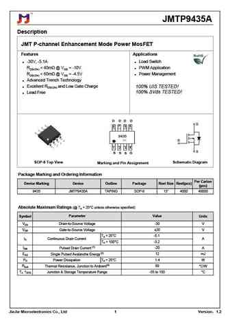
jmtp9435a.pdf
JMTP9435A Description JMT P-channel Enhancement Mode Power MosFET Features Applications -30V, -5.1A Load Switch RDS(ON) ... See More ⇒
jsm9435.pdf
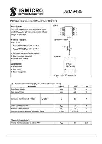
JSM9435 P-Channel Enhancement Mode Power MOSFET SOP-8 Description SD 1 8 The 9435 uses advanced trench technology to provide S D 2 7 excellent RDS(ON), low gate charge and operation with gate SD 3 6 G D 4 5 voltages as low as 4.5V. Top View Equivalent Cir cuit General Features S VDS = -30V = -4.2A RDS(ON) ... See More ⇒
lpm9435.pdf
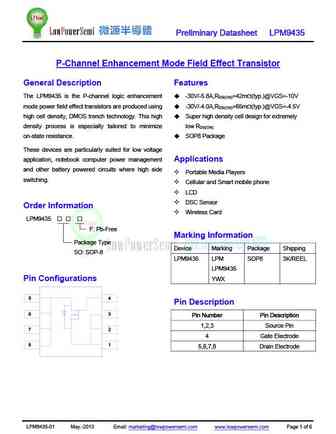
Preliminary Datasheet LPM9435 P-Channel Enhancement Mode Field Effect Transistor General Description Features The LPM9435 is the P-channel logic enhancement -30V/-5.8A,R =42m (typ.)@VGS=-10V DS(ON) mode power field effect transistors are produced using -30V/-4.0A,R =65m (typ.)@VGS=-4.5V DS(ON) high cell density, DMOS trench technology. This high Super high density ce... See More ⇒
si9435.pdf
SOP-8 Plastic-Encapsulate MOSFETS SI9435 P-Channel Enhancement Mode Power MOSFET SOP-8 Description SD 1 8 The SI9435 uses advanced trench technology to provide S D 2 7 excellent RDS(ON), low gate charge and operation with gate SD 3 6 G D 4 5 voltages as low as 4.5V. Top View Equivalent Cir cuit General Features S VDS = -30V = -4.2A RDS(ON) ... See More ⇒
pt9435.pdf
PT9435 -30V P-Channel Enhancement Mode MOSFET VDS= -30V RDS(ON), Vgs@-10V, Ids@-5.3A = 60m RDS(ON), Vgs@-4.5V, Ids@-4.2A = 95m Features Advanced trench process technology High Density Cell Design For Ultra Low On-Resistance Improved Shoot-Through FOM Package Dimensions Millimeter Millimeter REF. REF. Min. Max. Min. Max. A 5.80 6.20 M 0.10 0.25 B 4.80 5.00 H 0.31 0... See More ⇒
wsp9435.pdf
WSP9435 P-Ch MOSFET General Description Product Summery The WSP9435 is the highest performance trench BVDSS RDSON ID P-Ch MOSFET with extreme high cell density , which provide excellent RDSON and gate charge -30V 38m -5.4A for most of the synchronous buck converter applications . Applications The WSP9435 meet the RoHS and Green Product requirement , with full function re... See More ⇒
se9435.pdf
SHANGHAI August 2005 MICROELECTRONICS CO., LTD. SE9435 P-Channel Enhancement Mode Power MOSFET General Description Features The MOSFETs from SINO-IC provide the VDS = -30 V best combination of fast switching, low ID = -5.3 A on-resistance and cost-effectiveness. RDS(ON) = 0.050 @VGS = -10V Low gate charge. Fast switching speed. Applications Power management ... See More ⇒
sm9435.pdf
SM9435 P-Channel Enhancement-Mode MOSFET(-30V, -5.3A) PRODUCT SUMMARY VDSS ID RDS(on) (m-ohm) Max 60 @ VGS = -10 V, ID=-5.3A -30V -5.3A 90 @ VGS = -4.5V, ID=-4.2A Features 1 Advanced Trench Process Technology. 2 High Density Cell Design for Ultra Low On-Resistance. 3 Fully Characterized Avalanche Voltage and Current. 4 Improved Shoot-Through FOM. 5 RoHS ... See More ⇒
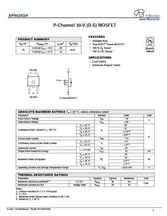
ut9435g.pdf
UT9435G www.VBsemi.tw P-Channel 30-V (D-S) MOSFET FEATURES PRODUCT SUMMARY Halogen-free VDS (V) RDS(on) ( ) ID (A)d Qg (Typ.) TrenchFET Power MOSFET 0.033 at VGS = - 10 V - 26 100 % Rg Tested RoHS - 30 19 nC COMPLIANT 100 % UIS Tested 0.046 at VGS = - 4.5 V - 21 APPLICATIONS Load Switch Notebook Adaptor Switch S TO-252 G G D S D Top View P-Cha... See More ⇒
ap9435gk.pdf
AP9435GK www.VBsemi.tw P-Channel 35 V (D-S) MOSFET FEATURES PRODUCT SUMMARY Halogen-free According to IEC 61249-2-21 VDS (V) RDS(on) ( ) ID (A)d Qg (Typ.) Definition 0.050 at VGS = - 10 V - 6.2 TrenchFET Power MOSFET - 35 9.8 nC 0.060 at VGS = - 4.5 V - 5.1 100 % Rg Tested 100 % UIS Tested Compliant to RoHS Directive 2002/95/EC S APPLICATIONS Load ... See More ⇒
vbza9435.pdf
VBZA9435 www.VBsemi.com P-Channel 30-V (D-S) MOSFET FEATURES PRODUCT SUMMARY Halogen-free VDS (V) RDS(on) ( ) ID (A)d Qg (Typ.) TrenchFET Power MOSFET 0.026at VGS = - 10 V - 6 100 % Rg Tested RoHS - 30 29 nC COMPLIANT 100 % UIS Tested 0.030 at VGS = - 4.5 V - 5 APPLICATIONS Load Switch Notebook Adaptor Switch SO-8 S S 1 8 D S D 2 7 G S 3 6 ... See More ⇒
fds9435a-nl.pdf

FDS9435A-NL www.VBsemi.tw P-Channel 30-V (D-S) MOSFET FEATURES PRODUCT SUMMARY Halogen-free According to IEC 61249-2-21 VDS (V) RDS(on) ( )ID (A) Definition 0.042 at VGS = - 10 V - 5.8 TrenchFET Power MOSFET 0.055 at VGS = - 6 V - 30 - 5.0 Compliant to RoHS Directive 2002/95/EC 0.060 at VGS = - 4.5 V - 4.4 S SO-8 G SD 1 8 S D 2 7 3 6 SD G D 4 5 D T... See More ⇒
apm9435kc.pdf
APM9435KC www.VBsemi.tw P-Channel 30-V (D-S) MOSFET FEATURES PRODUCT SUMMARY Halogen-free According to IEC 61249-2-21 VDS (V) RDS(on) ( )ID (A) Definition 0.042 at VGS = - 10 V - 5.8 TrenchFET Power MOSFET 0.055 at VGS = - 6 V - 30 - 5.0 Compliant to RoHS Directive 2002/95/EC 0.060 at VGS = - 4.5 V - 4.4 S SO-8 G SD 1 8 S D 2 7 3 6 SD G D 4 5 D Top... See More ⇒
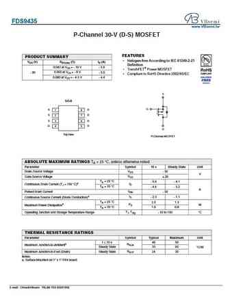
fds9435.pdf
FDS9435 www.VBsemi.tw P-Channel 30-V (D-S) MOSFET FEATURES PRODUCT SUMMARY Halogen-free According to IEC 61249-2-21 VDS (V) RDS(on) ( )ID (A) Definition 0.042 at VGS = - 10 V - 5.8 TrenchFET Power MOSFET 0.055 at VGS = - 6 V - 30 - 5.0 Compliant to RoHS Directive 2002/95/EC 0.060 at VGS = - 4.5 V - 4.4 S SO-8 G SD 1 8 S D 2 7 3 6 SD G D 4 5 D Top V... See More ⇒
ap9435k.pdf
AP9435K www.VBsemi.tw P-Channel 35 V (D-S) MOSFET FEATURES PRODUCT SUMMARY Halogen-free According to IEC 61249-2-21 VDS (V) RDS(on) ( ) ID (A)d Qg (Typ.) Definition 0.050 at VGS = - 10 V - 6.2 TrenchFET Power MOSFET - 35 9.8 nC 0.060 at VGS = - 4.5 V - 5.1 100 % Rg Tested 100 % UIS Tested Compliant to RoHS Directive 2002/95/EC S APPLICATIONS Load S... See More ⇒
si9435dy-t1.pdf

SI9435DY-T1 www.VBsemi.tw P-Channel 30-V (D-S) MOSFET FEATURES PRODUCT SUMMARY Halogen-free According to IEC 61249-2-21 VDS (V) RDS(on) ( )ID (A) Definition 0.042 at VGS = - 10 V - 5.8 TrenchFET Power MOSFET 0.055 at VGS = - 6 V - 30 - 5.0 Compliant to RoHS Directive 2002/95/EC 0.060 at VGS = - 4.5 V - 4.4 S SO-8 G SD 1 8 S D 2 7 3 6 SD G D 4 5 D T... See More ⇒
ssm9435gm.pdf
SSM9435GM www.VBsemi.tw P-Channel 30-V (D-S) MOSFET FEATURES PRODUCT SUMMARY Halogen-free According to IEC 61249-2-21 VDS (V) RDS(on) ( )ID (A) Definition 0.042 at VGS = - 10 V - 5.8 TrenchFET Power MOSFET 0.055 at VGS = - 6 V - 30 - 5.0 Compliant to RoHS Directive 2002/95/EC 0.060 at VGS = - 4.5 V - 4.4 S SO-8 G SD 1 8 S D 2 7 3 6 SD G D 4 5 D Top... See More ⇒
ap9435gm.pdf

AP9435GM www.VBsemi.tw P-Channel 30-V (D-S) MOSFET FEATURES PRODUCT SUMMARY Halogen-free According to IEC 61249-2-21 VDS (V) RDS(on) ( )ID (A) Definition 0.042 at VGS = - 10 V - 5.8 TrenchFET Power MOSFET 0.055 at VGS = - 6 V - 30 - 5.0 Compliant to RoHS Directive 2002/95/EC 0.060 at VGS = - 4.5 V - 4.4 S SO-8 G SD 1 8 S D 2 7 3 6 SD G D 4 5 D Top ... See More ⇒
si9435bdy-t1-e3.pdf
SI9435BDY-T1-E3 www.VBsemi.tw P-Channel 30-V (D-S) MOSFET FEATURES PRODUCT SUMMARY Halogen-free According to IEC 61249-2-21 VDS (V) RDS(on) ( )ID (A) Definition 0.042 at VGS = - 10 V - 5.8 TrenchFET Power MOSFET 0.055 at VGS = - 6 V - 30 - 5.0 Compliant to RoHS Directive 2002/95/EC 0.060 at VGS = - 4.5 V - 4.4 S SO-8 G SD 1 8 S D 2 7 3 6 SD G D 4 5 ... See More ⇒
me9435.pdf
ME9435 www.VBsemi.tw P-Channel 30-V (D-S) MOSFET FEATURES PRODUCT SUMMARY Halogen-free According to IEC 61249-2-21 VDS (V) RDS(on) ( )ID (A) Definition 0.042 at VGS = - 10 V - 5.8 TrenchFET Power MOSFET 0.055 at VGS = - 6 V - 30 - 5.0 Compliant to RoHS Directive 2002/95/EC 0.060 at VGS = - 4.5 V - 4.4 S SO-8 G SD 1 8 S D 2 7 3 6 SD G D 4 5 D Top Vi... See More ⇒
sdm9435a.pdf
SDM9435A www.VBsemi.tw P-Channel 30-V (D-S) MOSFET FEATURES PRODUCT SUMMARY Halogen-free According to IEC 61249-2-21 VDS (V) RDS(on) ( )ID (A) Definition 0.042 at VGS = - 10 V - 5.8 TrenchFET Power MOSFET 0.055 at VGS = - 6 V - 30 - 5.0 Compliant to RoHS Directive 2002/95/EC 0.060 at VGS = - 4.5 V - 4.4 S SO-8 G SD 1 8 S D 2 7 3 6 SD G D 4 5 D Top ... See More ⇒
nds9435a.pdf

NDS9435A www.VBsemi.tw P-Channel 30-V (D-S) MOSFET FEATURES PRODUCT SUMMARY Halogen-free According to IEC 61249-2-21 VDS (V) RDS(on) ( )ID (A) Definition 0.042 at VGS = - 10 V - 5.8 TrenchFET Power MOSFET 0.055 at VGS = - 6 V - 30 - 5.0 Compliant to RoHS Directive 2002/95/EC 0.060 at VGS = - 4.5 V - 4.4 S SO-8 G SD 1 8 S D 2 7 3 6 SD G D 4 5 D Top ... See More ⇒
ap9435gg.pdf
AP9435GG www.VBsemi.tw P-Channel 30-V (D-S) MOSFET FEATURES PRODUCT SUMMARY Halogen-free According to IEC 61249-2-21 VDS (V) RDS(on) ( ) ID (A)d Qg (Typ.) Definition 0.050 at VGS = - 10 V - 7.6 TrenchFET Power MOSFET - 30 13 nC 100 % Rg Tested 0.056 at VGS = - 4.5 V - 6.0 APPLICATIONS Load Switch Battery Switch D S G G D S D P-Channel MOSFET ABS... See More ⇒
ap9435gh.pdf
AP9435GH www.VBsemi.tw P-Channel 30-V (D-S) MOSFET FEATURES PRODUCT SUMMARY Halogen-free VDS (V) RDS(on) ( ) ID (A)d Qg (Typ.) TrenchFET Power MOSFET 0.033 at VGS = - 10 V - 26 100 % Rg Tested RoHS - 30 19 nC COMPLIANT 100 % UIS Tested 0.046 at VGS = - 4.5 V - 21 APPLICATIONS Load Switch Notebook Adaptor Switch S TO-252 G G D S D Top View P-Ch... See More ⇒
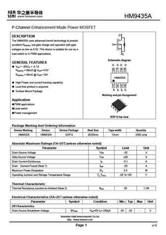
hm9435.pdf

HM9435 P-Channel Enhancement Mode Power MOSFET D DESCRIPTION The HM9435 uses advanced trench technology to provide G excellent RDS(ON), low gate charge and operation with gate voltages as low as 4.5V. This device is suitable for use as a load switch or in PWM applications. S Schematic diagram GENERAL FEATURES VDS = -30V,ID = -5.1A RDS(ON) ... See More ⇒
hm9435a.pdf
HM9435A P-Channel Enhancement Mode Power MOSFET D DESCRIPTION The HM9435A uses advanced trench technology to provide G excellent RDS(ON), low gate charge and operation with gate voltages as low as 4.5V. This device is suitable for use as a load switch or in PWM applications. S Schematic diagram GENERAL FEATURES VDS = -30V,ID = -5.1A RDS(ON) ... See More ⇒
hm9435b.pdf
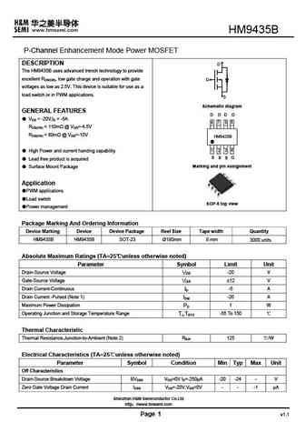
HM9435B P-Channel Enhancement Mode Power MOSFET DESCRIPTION D The HM9435B uses advanced trench technology to provide excellent RDS(ON), low gate charge and operation with gate G voltages as low as 2.5V. This device is suitable for use as a load switch or in PWM applications. S Schematic diagram GENERAL FEATURES VDS = -20V,ID = -5A RDS(ON) ... See More ⇒
ap9435a.pdf
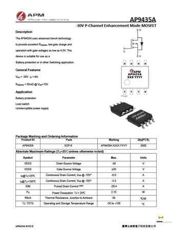
AP9435A -30V P-Channel Enhancement Mode MOSFET Description The AP9435A uses advanced trench technology to provide excellent R , low gate charge and DS(ON) operation with gate voltages as low as 4.5V. This device is suitable for use as a Battery protection or in other Switching application. General Features V = -30V I =-6A DS D R ... See More ⇒
Detailed specifications: 4835 , 4920 , 4946 , 4953 , 6604 , 8810 , 8820 , 8822 , AON6380 , 4953A , 4953B , 9926A , 9926B , AO3410 , APM2317 , FDMA905 , FDN338 .
History: 4946
Keywords - 9435 MOSFET specs
9435 cross reference
9435 equivalent finder
9435 pdf lookup
9435 substitution
9435 replacement
Need a MOSFET replacement? Our guide shows you how to find a perfect substitute by comparing key parameters and specs
History: 4946
🌐 : EN ES РУ

LIST
Last Update
MOSFET: ASB80R750E | ASB70R380E | ASB65R300E | ASB65R220E | ASB65R120EFD | ASB60R150E | ASA80R900E | ASA80R750E | ASA80R290E | ASA70R950E
Popular searches
sw50n06 | 2sa1232 | 2sc1940 | ftp08n06a | 2n3405 | 2n3567 | 2sc1226 | 2sd180