70N03 Specs and Replacement
Type Designator: 70N03
Type of Transistor: MOSFET
Type of Control Channel: N-Channel
Absolute Maximum Ratings
Pd ⓘ
- Maximum Power Dissipation: 68 W
|Vds|ⓘ - Maximum Drain-Source Voltage: 30 V
|Vgs|ⓘ - Maximum Gate-Source Voltage: 20 V
|Id| ⓘ - Maximum Drain Current: 70 A
Tj ⓘ - Maximum Junction Temperature: 175 °C
Electrical Characteristics
RDSonⓘ - Maximum Drain-Source On-State Resistance: 0.008 Ohm
Package: TO251
- MOSFET ⓘ Cross-Reference Search
70N03 datasheet
..1. Size:804K shenzhen
70n03.pdf 

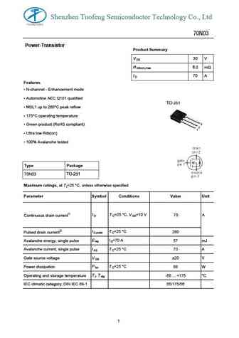
Shenzhen Tuofeng Semiconductor Technology Co., Ltd 70N03 Power-Transistor Product Summary V 30 V DS R 8.0 m DS(on),max I 70 A D Features N-channel - Enhancement mode Automotive AEC Q101 qualified TO-251 MSL1 up to 260 C peak reflow 175 C operating temperature 3 Green product (RoHS compliant) 2 1 Ultra low Rds(on) 100% Avalanche tested Ty... See More ⇒
..2. Size:2696K goford
70n03.pdf 

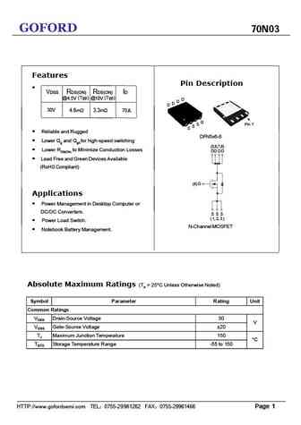
GOFORD 70N03 Features Pin Description VDSS RDS(ON) RDS(ON) ID @4.5V (Typ) @10V (Typ) D D D D 30V 4.6m 3.3m 70 A G Pin 1 S S S Reliable and Rugged DFN5x6-8 Lower Qg and Qgd for high-speed switching (5,6,7,8) Lower RDS(ON) to Minimize Conduction Losses DDDD Lead Free and Green Devices Available (RoHS Compliant) (4) G Applications Power Management in Deskto... See More ⇒
0.2. Size:1123K rohm
rxh070n03.pdf 

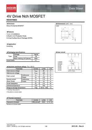
Data Sheet 4V Drive Nch MOSFET RXH070N03 Structure Dimensions (Unit mm) Silicon N-channel MOSFET SOP8 (8) (5) Features 1) Low on-resistance. 2) Built-in G-S Protection Diode. 3) Small Surface Mount Package (SOP8). (1) (4) Application Switching Packaging specifications Inner circuit (8) (7) (6) (5) Package Taping Type Code TB Basic ordering unit (pieces... See More ⇒
0.3. Size:73K vishay
sup70n03-09bp sub70n03-09bp.pdf 

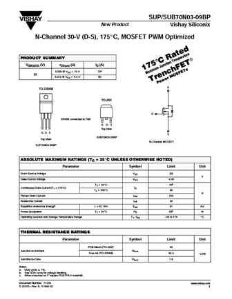
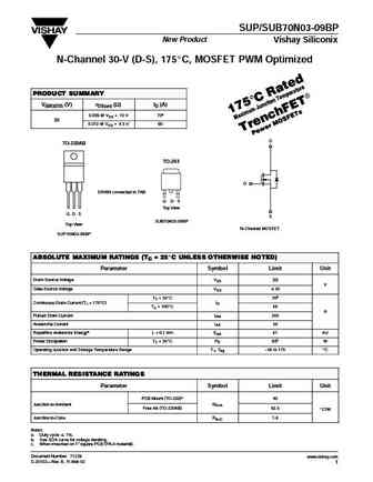
SUP/SUB70N03-09BP New Product Vishay Siliconix N-Channel 30-V (D-S), 175_C, MOSFET PWM Optimized PRODUCT SUMMARY V(BR)DSS (V) rDS(on) (W) ID (A) 0.009 @ VGS = 10 V 70a 30 0.013 @ VGS = 4.5 V 60 D TO-220AB TO-263 G DRAIN connected to TAB G D S Top View G D S S SUB70N03-09BP Top View N-Channel MOSFET SUP70N03-09BP ABSOLUTE MAXIMUM RATINGS (TC = 25_C UNLESS OTHERWISE NOTED) ... See More ⇒
0.4. Size:113K vishay
sup70n03-09p sub70n03-09p.pdf 

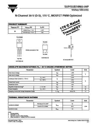
SUP/SUB70N03-09P Vishay Siliconix N-Channel 30-V (D-S), 175_C, MOSFET PWM Optimized PRODUCT SUMMARY V(BR)DSS (V) rDS(on) (W) ID (A) 0.009 @ VGS = 10 V "70a 30 30 0.015 @ VGS = 4.5 V "55 D TO-220AB TO-263 G DRAIN connected to TAB G D S Top View G D S S SUB70N03-09 Top View N-Channel MOSFET SUP70N03-09 ABSOLUTE MAXIMUM RATINGS (TC = 25_C UNLESS OTHERWISE NOTED) Parameter Sy... See More ⇒
0.5. Size:67K vishay
sum70n03-09cp.pdf 

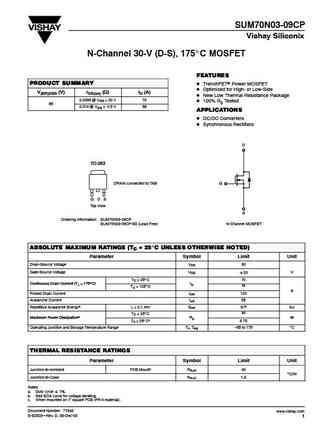
SUM70N03-09CP Vishay Siliconix N-Channel 30-V (D-S), 175_C MOSFET FEATURES PRODUCT SUMMARY D TrenchFETr Power MOSFET D Optimized for High- or Low-Side V(BR)DSS (V) rDS(on) (W) ID (A) D New Low Thermal Resistance Package 0.0095 @ VGS = 20 V 70 D 100% Rg Tested 30 30 0.014 @ VGS = 4.5 V 58 APPLICATIONS D DC/DC Converters D Synchronous Rectifiers D TO-263 DRAIN connected to TAB ... See More ⇒
0.6. Size:52K vishay
sup70n03-09bp.pdf 

SUP/SUB70N03-09BP New Product Vishay Siliconix N-Channel 30-V (D-S), 175_C, MOSFET PWM Optimized PRODUCT SUMMARY V(BR)DSS (V) rDS(on) (W) ID (A) 0.009 @ VGS = 10 V 70a 30 0.013 @ VGS = 4.5 V 60 D TO-220AB TO-263 G DRAIN connected to TAB G D S Top View G D S S SUB70N03-09BP Top View N-Channel MOSFET SUP70N03-09BP ABSOLUTE MAXIMUM RATINGS (TC = 25_C UNLESS OTHERWISE NOTED) ... See More ⇒
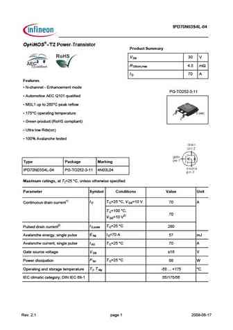
0.7. Size:186K infineon
ipd70n03s4l-04.pdf 

IPD70N03S4L-04 OptiMOS -T2 Power-Transistor Product Summary V 30 V DS R 4.3 m DS(on),max I 70 A D Features N-channel - Enhancement mode PG-TO252-3-11 Automotive AEC Q101 qualified MSL1 up to 260 C peak reflow 175 C operating temperature Green product (RoHS compliant) Ultra low Rds(on) 100% Avalanche tested Type Package Marking IPD70N03S4L-04... See More ⇒
0.8. Size:186K infineon
ipd70n03s4l-04 ds.pdf 

IPD70N03S4L-04 OptiMOS -T2 Power-Transistor Product Summary V 30 V DS R 4.3 m DS(on),max I 70 A D Features N-channel - Enhancement mode PG-TO252-3-11 Automotive AEC Q101 qualified MSL1 up to 260 C peak reflow 175 C operating temperature Green product (RoHS compliant) Ultra low Rds(on) 100% Avalanche tested Type Package Marking IPD70N03S4L-04... See More ⇒
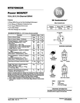
0.9. Size:85K onsemi
ntd70n03r-001 ntd70n03rg ntd70n03r.pdf 

NTD70N03R Power MOSFET 72 A, 25 V, N-Channel DPAK Features Planar HD3e Process for Fast Switching Performance http //onsemi.com Low RDS(on) to Minimize Conduction Loss Low CISS to Minimize Driver Loss V(BR)DSS RDS(on) TYP ID MAX Low Gate Charge 25 V 5.6 mW 72 A Pb-Free Packages are Available N-Channel MAXIMUM RATINGS (TJ = 25 C Unless otherwise specified) D P... See More ⇒
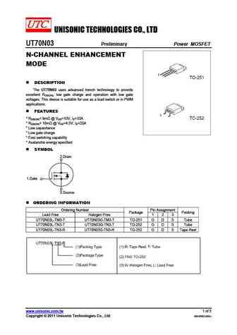
0.10. Size:146K utc
ut70n03.pdf 

UNISONIC TECHNOLOGIES CO., LTD UT70N03 Preliminary Power MOSFET N-CHANNEL ENHANCEMENT MODE DESCRIPTION The UT70N03 uses advanced trench technology to provide excellent RDS(ON), low gate charge and operation with low gate voltages. This device is suitable for use as a load switch or in PWM applications. FEATURES * RDS(ON)... See More ⇒
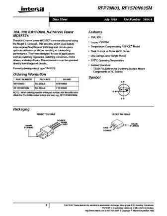
0.11. Size:142K intersil
rfp70n03 rf1s70n03sm.pdf 

RFP70N03, RF1S70N03SM Data Sheet July 1999 File Number 3404.4 70A, 30V, 0.010 Ohm, N-Channel Power Features MOSFETs 70A, 30V These N-Channel power MOSFETs are manufactured using rDS(ON) = 0.010 the MegaFET process. This process, which uses feature Temperature Compensating PSPICE Model sizes approaching those of LSI integrated circuits gives optimum utilization of sili... See More ⇒
0.12. Size:676K secos
ssd70n03-04d.pdf 

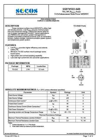
SSD70N03-04D 75A, 30V, RDS(ON) 6 m N-Ch Enhancement Mode Power MOSFET Elektronische Bauelemente RoHS Compliant Product A suffix of -C specifies halogen free TO-252(D-Pack) DESCRIPTION These miniature surface mount MOSFETs utilize high cell density process. Low RDS(on) assures minimal power loss and conserves energy, making this device ideal for use in power manageme... See More ⇒
0.13. Size:2356K jiangsu
cjac70n03.pdf 

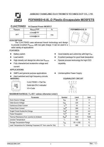
JIANGSU CHANGJING ELECTRONICS TECHNOLOGY CO., LTD PDFNWB5 6-8L-D Plastic-Encapsulate MOSFETS CJAC70N03 N-Channel Power MOSFET V(BR)DSS ID RDS(on)TYP PDFN 5 6-8L-D 4.3m @10V 30 V 70A 6.0m @4.5V DESCRIPTION The CJAC70N03 uses advanced trench technology and design to provide excellent RDS(ON) with low gate charge. It can be used in a wide variety of applications FEATURE... See More ⇒
0.14. Size:302K analog power
am70n03-04d.pdf 

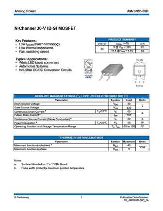
Analog Power AM70N03-04D N-Channel 30-V (D-S) MOSFET PRODUCT SUMMARY Key Features rDS(on) (m ) VDS (V) ID(A) Low r trench technology DS(on) 6 @ VGS = 10V 75 Low thermal impedance 30 8 @ VGS = 4.5V 65 Fast switching speed Typical Applications White LED boost converters Automotive Systems Industrial DC/DC Conversion Circuits ABSOLUTE MAXIMUM R... See More ⇒
0.15. Size:302K analog power
am70n03-08d.pdf 

Analog Power AM70N03-08D N-Channel 30-V (D-S) MOSFET PRODUCT SUMMARY Key Features rDS(on) (m ) VDS (V) ID(A) Low r trench technology DS(on) 8 @ VGS = 10V 65 Low thermal impedance 30 11.5 @ VGS = 4.5V 54 Fast switching speed Typical Applications White LED boost converters Automotive Systems Industrial DC/DC Conversion Circuits ABSOLUTE MAXIMU... See More ⇒
0.16. Size:906K blue-rocket-elect
bri70n03.pdf 

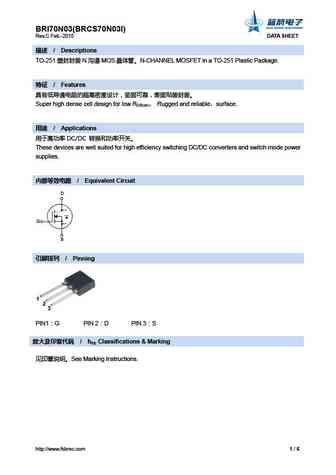
BRI70N03(BRCS70N03I) Rev.C Feb.-2015 DATA SHEET / Descriptions TO-251 N MOS N-CHANNEL MOSFET in a TO-251 Plastic Package. / Features Super high dense cell design for low RDS(on) Rugged and reliable surface. / Applications DC/... See More ⇒
0.19. Size:847K blue-rocket-elect
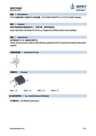
brd70n03.pdf 

BRD70N03 Rev.E Dec.-2017 DATA SHEET / Descriptions TO-252 N MOS N-CHANNEL MOSFET in a TO-252 Plastic Package. / Features Super high dense cell design for low RDS(on),Rugged and reliable,surface mount package. / Applications DC/... See More ⇒
0.20. Size:692K shantou-huashan
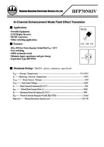
hfp70n03v.pdf 

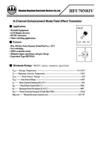
Shantou Huashan Electronic Devices Co.,Ltd. HFP70N03V N-Channel Enhancement Mode Field Effect Transistor Applications TO-220 Portable Equipment. LCD Display Inverter. DC/DC converters Other switching applications. 1- G 2-D 3-S Features 50A, 30V(See Note), RDS(on) ... See More ⇒
0.21. Size:691K shantou-huashan
hfu70n03v.pdf 

Shantou Huashan Electronic Devices Co.,Ltd. HFU70N03V N-Channel Enhancement Mode Field Effect Transistor Applications TO-251 Portable Equipment. LCD Display Inverter. DC/DC converters Other switching applications. 1- G 2-D 3-S Features 50A, 30V(See Note), RDS(on) ... See More ⇒
0.22. Size:1184K kexin
ndt70n03.pdf 

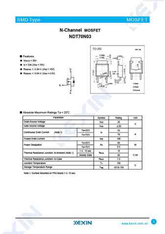
SMD Type MOSFET N-Channel MOSFET NDT70N03 TO-252 Unit mm +0.15 6.50-0.15 +0.1 2.30 -0.1 Features +0.2 5.30-0.2 +0.8 0.50 -0.7 VDS (V) = 30V ID = 33A (VGS = 10V) RDS(ON) 4.3m (VGS = 10V) D 0.127 +0.1 0.80-0.1 RDS(ON) 6.5m (VGS = 4.5V) max + 0.1 1 Gate 2.3 0.60- 0.1 G +0.15 4.60 -0.15 2 Drain 3 Source S Absolute Maximum Ratings... See More ⇒
0.23. Size:362K bruckewell
ms70n03.pdf 

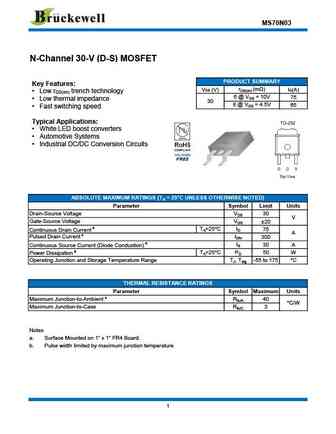
MS70N03 N-Channel 30-V (D-S) MOSFET PRODUCT SUMMARY Key Features rDS(on) (m ) VDS (V) ID(A) Low r trench technology DS(on) 6 @ VGS = 10V 75 Low thermal impedance 30 8 @ VGS = 4.5V 65 Fast switching speed Typical Applications White LED boost converters Automotive Systems Industrial DC/DC Conversion Circuits ABSOLUTE MAXIMUM RATINGS (TA = 25 C UNLE... See More ⇒
0.24. Size:708K feihonltd
fhu70n03a fhd70n03a.pdf 

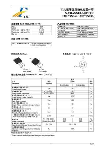
N N-CHANNEL MOSFET FHU70N03A/FHD70N03A MAIN CHARACTERISTICS FEATURES ID 68 A Low gate charge VDSS 30 V Crss ( 130pF) Low Crss (typical 130pF ) Rdson-typ @Vgs=10V 7.4m Fast switching Rdson-typ @Vgs=4.5V 10.8m 100% 100% avalanche tested ... See More ⇒
0.25. Size:1428K matsuki electric
me70n03s me70n03s-g.pdf 

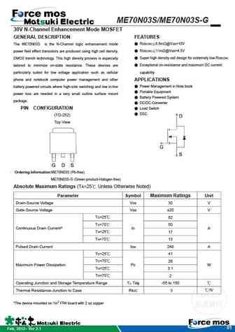
ME70N03S/ME70N03S-G 30V N-Channel Enhancement Mode MOSFET GENERAL DESCRIPTION FEATURES RDS(ON) 6.6m @VGS=10V The ME70N03S is the N-Channel logic enhancement mode RDS(ON) 11m @VGS=4.5V power field effect transistors are produced using high cell density, Super high density cell design for extremely low RDS(ON) DMOS trench technology. This high density process is ... See More ⇒
0.26. Size:898K cn hunteck
htj270n03.pdf 

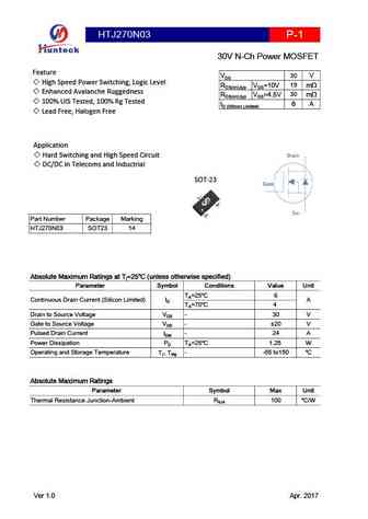
HTJ270N03 P-1 30V N-Ch Power MOSFET Feature 30 V VDS High Speed Power Switching, Logic Level 19 RDS(on),typ VGS=10V m Enhanced Avalanche Ruggedness 30 RDS(on),typ VGS=4.5V m 100% UIS Tested, 100% Rg Tested 6 A ID (Sillicon Limited) Lead Free, Halogen Free Application Hard Switching and High Speed Circuit Drain DC/DC in Telecoms and Inductrial SOT... See More ⇒
0.27. Size:2026K cn vbsemi
vbzl70n03.pdf 

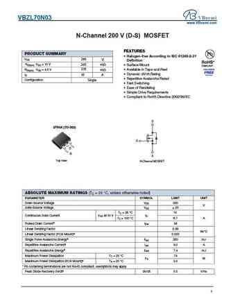
VBZL70N03 www.VBsemi.com N-Channel 200 V (D-S) MOSFET FEATURES PRODUCT SUMMARY Halogen-free According to IEC 61249-2-21 VDS 200 V Definition RDS(on) VGS = 10 V 260 m Surface Mount 370 Available in Tape and Reel RDS(on) VGS = 4.5 V m Dynamic dV/dt Rating ID 10 A Repetitive Avalanche Rated Configuration Single Fast Switching Ease of Paralleling ... See More ⇒
0.28. Size:1220K cn vbsemi
vbzfb70n03.pdf 

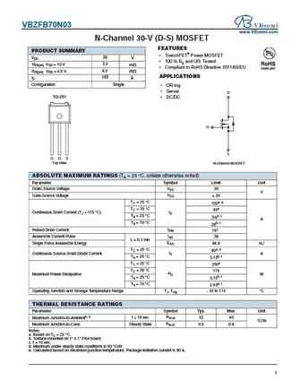
VBZFB70N03 www.VBsemi.com N-Channel 30-V (D-S) MOSFET FEATURES PRODUCT SUMMARY TrenchFET Power MOSFET VDS 30 V 100 % Rg and UIS Tested 3.5 RDS(on) VGS = 10 V m Compliant to RoHS Directive 2011/65/EU RDS(on) VGS = 4.5 V 4.5 m APPLICATIONS 100 ID A Configuration Single OR-ing Server D TO-251 DC/DC G S G D S Top View N-Channel MOSFET ... See More ⇒
0.29. Size:1442K cn vbsemi
vbze70n03.pdf 

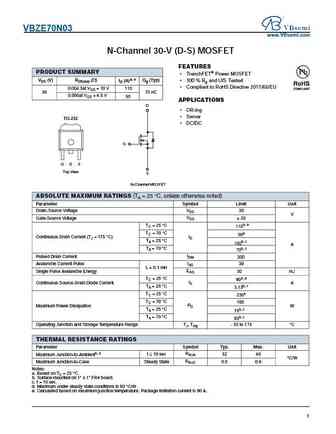
VBZE70N03 www.VBsemi.com N-Channel 30-V (D-S) MOSFET FEATURES PRODUCT SUMMARY TrenchFET Power MOSFET VDS (V) RDS(on) ( ) ID (A)a, e Qg (Typ) 100 % Rg and UIS Tested Compliant to RoHS Directive 2011/65/EU 0.004.5at VGS = 10 V 110 30 70 nC 0.006at VGS = 4.5 V 98 APPLICATIONS D OR-ing Server TO-252 DC/DC G G D S Top View S N-Channel MOSFET AB... See More ⇒
0.30. Size:620K cn hmsemi
hms170n03d.pdf 

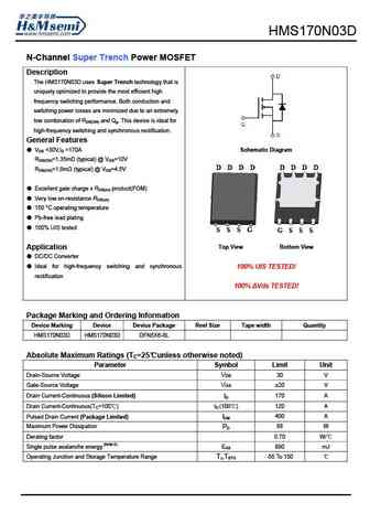
HMS170N03D N-Channel Super Trench Power MOSFET Description The HMS170N03D uses Super Trench technology that is uniquely optimized to provide the most efficient high frequency switching performance. Both conduction and switching power losses are minimized due to an extremely low combination of RDS(ON) and Qg. This device is ideal for high-frequency switching and synchronous rectif... See More ⇒
0.31. Size:515K cn minos
mdt70n03.pdf 

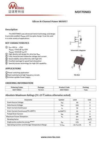
Silicon N-Channel Power MOSFET Description The MDT70N03 uses advanced trench technology and design to provide excellent R with low gate charge. It can be used DS(ON) in a wide variety of applications. KEY CHARACTERISTICS V =30V,I =70A DS D R ... See More ⇒
0.32. Size:205K inchange semiconductor
rfp70n03.pdf 
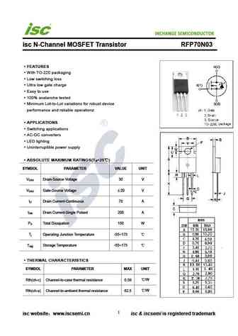
INCHANGE Semiconductor isc N-Channel MOSFET Transistor RFP70N03 FEATURES With TO-220 packaging Low switching loss Ultra low gate charge Easy to use 100% avalanche tested Minimum Lot-to-Lot variations for robust device performance and reliable operationz APPLICATIONS Switching applications AC-DC converters LED lighting Uninterruptible power supply ABSOLUT... See More ⇒
0.33. Size:4048K cn apm
ap70n03df.pdf 

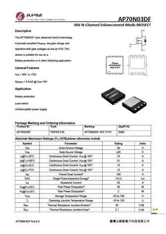
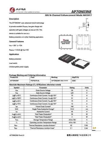
AP70N03DF 30V N-Channel Enhancement Mode MOSFET Description The AP70N03DF uses advanced trench technology to provide excellent R , low gate charge and DS(ON) operation with gate voltages as low as 4.5V. This device is suitable for use as a Battery protection or in other Switching application. General Features V = 30V I =70A DS D R ... See More ⇒
0.34. Size:2676K cn apm
ap70n03nf.pdf 

AP70N03NF 30V N-Channel Enhancement Mode MOSFET Description The AP70N03NF uses advanced trench technology to provide excellent R , low gate charge and DS(ON) operation with gate voltages as low as 4.5V. This device is suitable for use as a Battery protection or in other Switching application. General Features V = 30V I =70A DS D R ... See More ⇒
Detailed specifications: SI2319
, SI2323
, SI2328
, SIA519
, XP151A13AO
, XP152A12CO
, 20N06
, 60N03
, IRFB31N20D
, 90N03
, SSS10N60
, SSS12N60
, SSS1N60
, SSS2N60
, SSS5N60
, SSS7N60
, SSS8N60
.
History: IRFIB41N15D
| WMM07N65C2
Keywords - 70N03 MOSFET specs
70N03 cross reference
70N03 equivalent finder
70N03 pdf lookup
70N03 substitution
70N03 replacement
Step-by-step guide to finding a MOSFET replacement. Cross-reference parts and ensure compatibility for your repair or project.
