SSS2N60 Specs and Replacement
Type Designator: SSS2N60
Type of Transistor: MOSFET
Type of Control Channel: N-Channel
Absolute Maximum Ratings
Pd ⓘ - Maximum Power Dissipation: 45 W
|Vds|ⓘ - Maximum Drain-Source Voltage: 600 V
|Vgs|ⓘ - Maximum Gate-Source Voltage: 30 V
|Id| ⓘ - Maximum Drain Current: 2 A
Tj ⓘ - Maximum Junction Temperature: 150 °C
Electrical Characteristics
RDSonⓘ - Maximum Drain-Source On-State Resistance: 5 Ohm
SSS2N60 substitution
- MOSFET ⓘ Cross-Reference Search
SSS2N60 datasheet
sss2n60.pdf
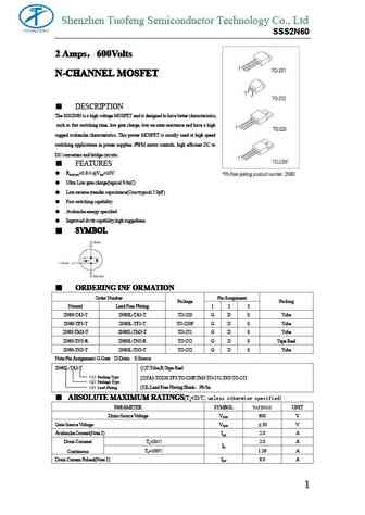
Shenzhen Tuofeng Semiconductor Technology Co., Ltd SSS2N60 2 Amps 600Volts 2 Amps 600Volts 2 Amps 600Volts 2 Amps 600Volts N-CHANNEL MOSFET N-CHANNEL MOSFET N-CHANNEL MOSFET N-CHANNEL MOSFET DESCRIPTION The SSS2N60 is a high voltage MOSFET and is designed to have better characteristics, such as fast switching time, low gate charge, low on-state resistance and have a high rug... See More ⇒
sss2n60.pdf
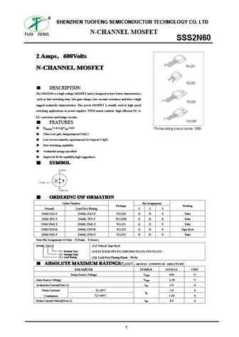
SHENZHEN TUOFENG SEMICONDUCTOR TECHNOLOGY CO. LTD N-CHANNEL MOSFET SSS2N60 2 Amps 600Volts 2 Amps 600Volts 2 Amps 600Volts 2 Amps 600Volts N-CHANNEL MOSFET N-CHANNEL MOSFET N-CHANNEL MOSFET N-CHANNEL MOSFET DESCRIPTION The SSS2N60 is a high voltage MOSFET and is designed to have better characteristics, such as fast switching time, low gate charge, low on-state resistance and... See More ⇒
ssp2n60b sss2n60b.pdf
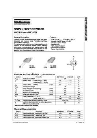
SSP2N60B/SSS2N60B 600V N-Channel MOSFET General Description Features These N-Channel enhancement mode power field effect 2.0A, 600V, RDS(on) = 5.0 @VGS = 10 V transistors are produced using Fairchild s proprietary, Low gate charge ( typical 12.5 nC) planar, DMOS technology. Low Crss ( typical 7.6 pF) This advanced technology has been especially tailored to Fast swit... See More ⇒
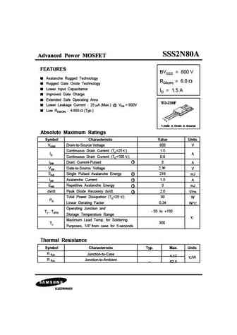
sss2n60a.pdf

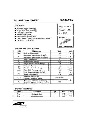
Advanced Power MOSFET FEATURES BVDSS = 600 V Avalanche Rugged Technology RDS(on) = 5 Rugged Gate Oxide Technology Lower Input Capacitance ID = 1.3 A Improved Gate Charge Extended Safe Operating Area Lower Leakage Current 25 A (Max.) @ VDS = 600V Lower RDS(ON) 3.892 (Typ.) 1 2 3 1.Gate 2. Drain 3. Source Absolute Maximum Ratings Symbol Characteristic Valu... See More ⇒
Detailed specifications: XP152A12CO , 20N06 , 60N03 , 70N03 , 90N03 , SSS10N60 , SSS12N60 , SSS1N60 , IRFZ46N , SSS5N60 , SSS7N60 , SSS8N60 , 1002 , 1115 , 1515 , G1601 , 2300 .
Keywords - SSS2N60 MOSFET specs
SSS2N60 cross reference
SSS2N60 equivalent finder
SSS2N60 pdf lookup
SSS2N60 substitution
SSS2N60 replacement
Learn how to find the right MOSFET substitute. A guide to cross-reference, check specs and replace MOSFETs in your circuits.
🌐 : EN ES РУ

LIST
Last Update
MOSFET: ASB80R750E | ASB70R380E | ASB65R300E | ASB65R220E | ASB65R120EFD | ASB60R150E | ASA80R900E | ASA80R750E | ASA80R290E | ASA70R950E
Popular searches
ksa1015yta | 2n4240 | 2n5210 transistor | toshiba 2sc2290 | pk6d0ba mosfet | 2sd726 | c536 transistor equivalent | 2sa1294 datasheet