2300 Datasheet. Specs and Replacement
Type Designator: 2300 📄📄
Type of Transistor: MOSFET
Type of Control Channel: N-Channel
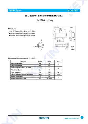
Absolute Maximum Ratings
Pd ⓘ - Maximum Power Dissipation: 1.25 W
|Vds|ⓘ - Maximum Drain-Source Voltage: 20 V
|Vgs|ⓘ - Maximum Gate-Source Voltage: 12 V
|Id| ⓘ - Maximum Drain Current: 5.2 A
Tj ⓘ - Maximum Junction Temperature: 150 °C
Electrical Characteristics
tr ⓘ - Rise Time: 46 nS
Cossⓘ - Output Capacitance: 150 pF
RDSonⓘ - Maximum Drain-Source On-State Resistance: 0.032 Ohm
Package: SOT23
📄📄 Copy
2300 substitution
- MOSFET ⓘ Cross-Reference Search
2300 datasheet
2300.pdf
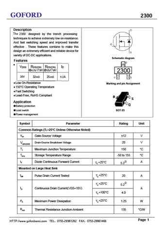
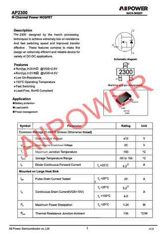
GOFORD 2300 Description The 2300 designed by the trench processing techniques to achieve extremely low on-resistance. And fast switching speed and improved transfer effective . These features combine to make this design an extremely efficient and reliable device for variety of DC-DC applications. Schematic diagram Features VDSS RDS(ON) RDS(ON) ID @4.5V (Typ) @10V (Ty... See More ⇒
2300.pdf
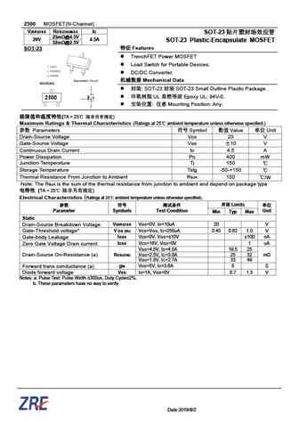
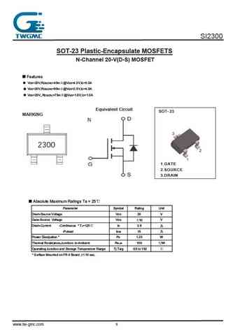
2300 MOSFET(N-Channel) V(BR)DSS RDS(ON)MAX ID SOT-23 25m @4.5V 20V 4.5A SOT-23 Plastic-Encapsulate MOSFET 32m @2.5V SOT-23 Features TrenchFET Power MOSFET Load Switch for Portable Devices. DC/DC Converter. Mechanical Data SOT-23 SOT-23 Small Outline Plastic Package. UL Epoxy ... See More ⇒
bm2300.pdf
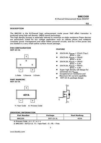
BM2300 N Channel Enhancement Mode MOSFET 4A DESCRIPTION The BM2300 is the N-Channel logic enhancement mode power field effect transistor is produced using high cell density, DMOS trench technology. This high density process is especially tailored to minimize on-state resistance.These devices are particularly suited for low voltage application such as cellular phone and notebook ... See More ⇒
ptb23006u 2.pdf
DISCRETE SEMICONDUCTORS DATA SHEET PTB23006U Microwave power transistor 1997 Feb 19 Preliminary specification Supersedes data of December 1994 Philips Semiconductors Preliminary specification Microwave power transistor PTB23006U FEATURES QUICK REFERENCE DATA Microwave performance up to Tmb =25 C in a common-base class C Very high power gain narrowband amplifier. Diffused ... See More ⇒
ptb23002u 2.pdf
DISCRETE SEMICONDUCTORS DATA SHEET PTB23002U NPN microwave power transistor 1997 Feb 19 Product specification Supersedes data of November 1994 Philips Semiconductors Product specification NPN microwave power transistor PTB23002U FEATURES QUICK REFERENCE DATA Microwave performance up to Tmb =25 C in a common-base class C Very high power gain narrowband amplifier. Internal ... See More ⇒
ptb23003x 3.pdf
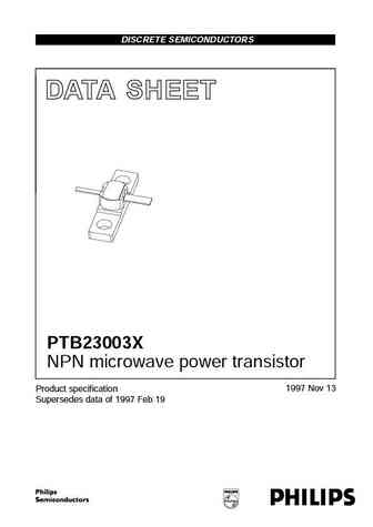
DISCRETE SEMICONDUCTORS DATA SHEET handbook, halfpage M3D031 PTB23003X NPN microwave power transistor 1997 Nov 13 Product specification Supersedes data of 1997 Feb 19 Philips Semiconductors Product specification NPN microwave power transistor PTB23003X FEATURES PINNING - SOT440A Diffused emitter ballasting resistors providing excellent PIN DESCRIPTION current sharing and with... See More ⇒
phc2300.pdf
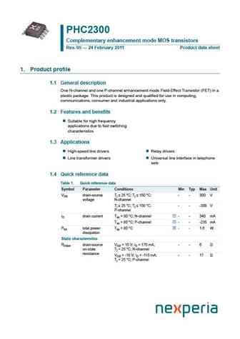
PHC2300 Complementary enhancement mode MOS transistors Rev. 05 24 February 2011 Product data sheet 1. Product profile 1.1 General description One N-channel and one P-channel enhancement mode Field-Effect Transistor (FET) in a plastic package. This product is designed and qualified for use in computing, communications, consumer and industrial applications only. 1.2 Features and ben... See More ⇒
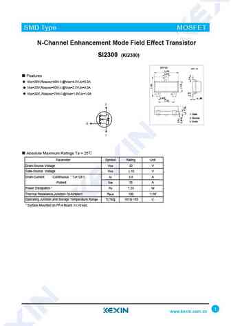
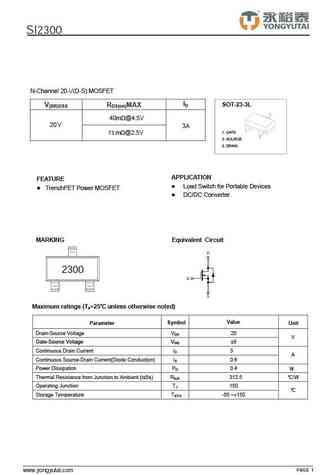
si2300ds.pdf
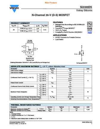
New Product Si2300DS Vishay Siliconix N-Channel 30-V (D-S) MOSFET FEATURES PRODUCT SUMMARY Halogen-free According to IEC 61249-2-21 VDS (V) RDS(on) ( ) Qg (Typ.) ID (A) Definition 0.068 at VGS = 4.5 V TrenchFET Power MOSFET 3.6a 30 3 nC 100 % Rg Tested 0.085 at VGS = 2.5 V 3.4 Compliant to RoHS Directive 2002/95/EC APPLICATIONS DC/DC Converter for ... See More ⇒
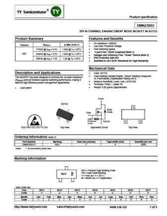
dmn2300ufb4.pdf
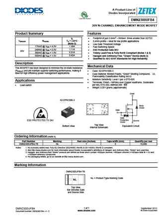
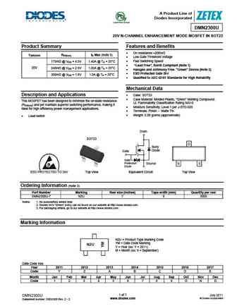
A Product Line of Diodes Incorporated DMN2300UFB4 20V N-CHANNEL ENHANCEMENT MODE MOSFET Product Summary Features Footprint of just 0.6mm2 thirteen times smaller than SOT23 ID V(BR)DSS RDS(ON) TA = +25 C 0.4mm profile ideal for low profile applications (Note 5) Low Gate Threshold Voltage 175m @ VGS = 4.5V 1.30A Fast Switching Speed 240m @ VGS =... See More ⇒
dmn2300ufd.pdf
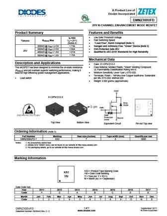
A Product Line of Diodes Incorporated DMN2300UFD 20V N-CHANNEL ENHANCEMENT MODE MOSFET Product Summary Features and Benefits Low Gate Threshold Voltage ID max Fast Switching Speed V(BR)DSS RDS(on) Max TA = 25 C (Notes 4) Lead Free , RoHS Compliant (Note 1) 200m @ VGS = 4.5V 1.73A Halogen and Antimony Free. "Green" Device (Note 2) 260m @ VGS = 2.5V ... See More ⇒
dmn2300ufl4.pdf
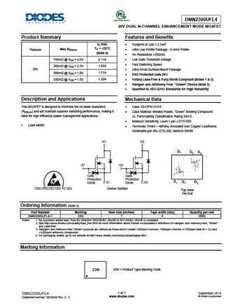
DMN2300UFL4 20V DUAL N-CHANNEL ENHANCEMENT MODE MOSFET Product Summary Features and Benefits ID max Footprint of Just 1.3 mm2 TA = +25 C V(BR)DSS Max RDS(on) Ultra Low Profile Package - 0.4mm Profile (Note 6) On Resistance ... See More ⇒
sil2300.pdf
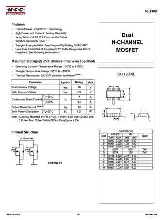
SIL2300 Features Trench Power LV MOSFET Technology High Power and Current Handing Capability Dual Epoxy Meets UL 94 V-0 Flammability Rating Moisture Sensitivity Level 1 N-CHANNEL Halogen Free Available Upon Request By Adding Suffix "-HF" Lead Free Finish/RoHS Compliant ("P" Suffix Designates RoHS MOSFET Compliant. See Ordering Information) Maximum Ratings@ 25... See More ⇒
fc8v22300l.pdf
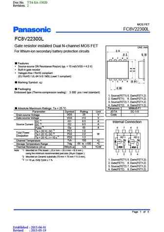
Doc No. TT4-EA-15020 Revision. 2 Product Standards MOS FET FC8V22300L FC8V22300L Gate resistor installed Dual N-channel MOS FET Unit mm 2.9 For lithium-ion secondary battery protection circuits 0.3 0.16 8 7 6 5 Features Source-source ON Resistance Rss(on) typ. = 15 mW VGS = 4.5 V) Built-in gate resistor Halogen-free / RoHS compliant (EU RoHS / UL-94 V-0 / MSL ... See More ⇒
mrf6v2300n.pdf
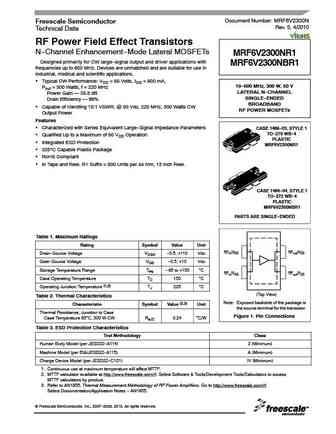
Document Number MRF6V2300N Freescale Semiconductor Rev. 5, 4/2010 Technical Data RF Power Field Effect Transistors N--Channel Enhancement--Mode Lateral MOSFETs MRF6V2300NR1 Designed primarily for CW large--signal output and driver applications with MRF6V2300NBR1 frequencies up to 600 MHz. Devices are unmatched and are suitable for use in industrial, medical and scientific application... See More ⇒
2sd2300.pdf
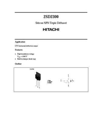
2SD2300 Silicon NPN Triple Diffused Application CTV horizontal deflection output Features High breakdown voltage VCBO = 1500 V Built-in damper diode type Outline TO-3PFM 2 1 1. Base ID 2. Collector 3. Emitter 1 3 2 3 2SD2300 Absolute Maximum Ratings (Ta = 25 C) Item Symbol Ratings Unit Collector to emitter voltage VCES 1500 V Emitter to base voltage VEBO 6V ... See More ⇒
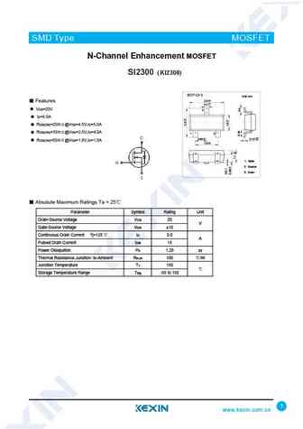
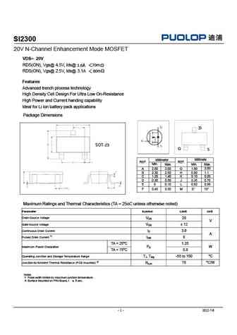
si2300.pdf
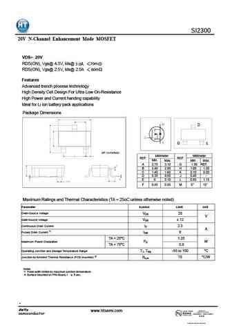
SI2300 20V N-Channel Enhancement Mode MOSFET VDS= 20V RDS(ON), Vgs@ 4.5V, Ids@ 3.0A 70m RDS(ON), Vgs@ 2.5V, Ids@ 2.0A 80m Features Advanced trench process technology High Density Cell Design For Ultra Low On-Resistance High Power and Current handing capability Ideal for Li ion battery pack applications Package Dimensions D G S SOT-23(PACKAGE) Millimeter Millime... See More ⇒
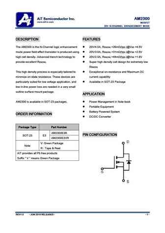
am2300n.pdf
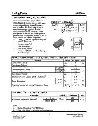
Analog Power AM2300N N-Channel 20-V (D-S) MOSFET These miniature surface mount MOSFETs PRODUCT SUMMARY utilize High Cell Density process. Low rDS(on) assures minimal power loss and conserves VDS (V) rDS(on) ( )ID (A) energy, making this device ideal for use in 0.035 @ VGS = 4.5V 4.3 20 power management circuitry. Typical 0.050 @ VGS = 2.5V 3.5 applications are DC-DC converters, ... See More ⇒
si2300.pdf
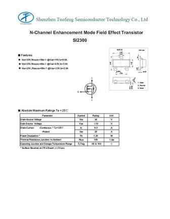
Shenzhen Tuofeng Semiconductor Technology Co., Ltd SMD Type IC SMD Type MOSFET N-Channel Enhancement Mode Field Effect Transistor SI2300 SOT-23 Unit mm +0.1 2.9-0.1 +0.1 0.4-0.1 Features 3 V DS=20V,RDS(ON)=30m @VGS=10V,ID=6.0A V DS=20V,RDS(ON)=40m @VGS=4.5V,ID=3.0A V DS=20V,,RDS(ON)=55m @V GS=2.5V,ID=2.0A 12 +0.1 +0.05 0.95-0.1 0.1-0.01 +0.1 1.9-0.1 1.Base 1. Gate 2.Emi... See More ⇒
mtn2300n3.pdf
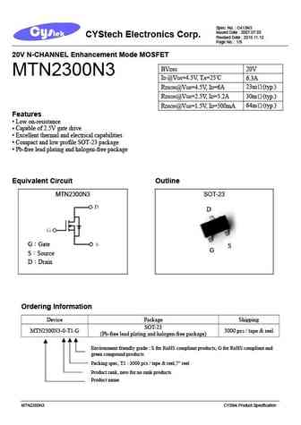
Spec. No. C413N3 Issued Date 2007.07.05 CYStech Electronics Corp. Revised Date 2015.11.12 Page No. 1/9 20V N-CHANNEL Enhancement Mode MOSFET BVDSS 20V MTN2300N3 ID @VGS=4.5V, TA=25 C 6.3A 23m (typ.) RDSON@VGS=4.5V, ID=6A 30m (typ.) RDSON@VGS=2.5V, ID=5.2A 64m (typ.) RDSON@VGS=1.5V, ID=500mA Features Low on-resistance Capable of 2.5V gate dr... See More ⇒
mtn2300an3.pdf
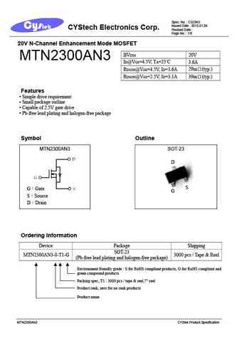
Spec. No. C323N3 Issued Date 2015.01.06 CYStech Electronics Corp. Revised Date Page No. 1/8 20V N-Channel Enhancement Mode MOSFET BVDSS 20V MTN2300AN3 ID@VGS=4.5V, TA=25 C 3.6A 29m (typ.) RDSON@VGS=4.5V, ID=3.6A 39m (typ.) RDSON@VGS=2.5V, ID=3.1A Features Simple drive requirement Small package outline Capable of 2.5V gate drive Pb-fr... See More ⇒
2300f.pdf
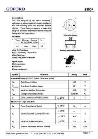
GOFORD 2300F Description The 2300F designed by the trench processing techniques to achieve extremely low on-resistance. And fast switching speed and improved transfer effective . These features combine to make this design an extremely efficient and reliable device for variety of DC-DC applications. Schematic diagram Features VDSS RDS(ON) RDS(ON) ID @4.5V (Typ) @2.5V ... See More ⇒
sts2300s.pdf
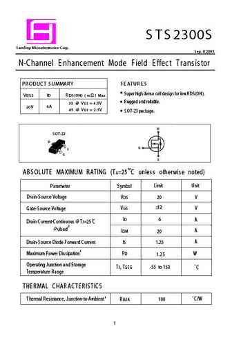
S TS 2300S S amHop Microelectronics C orp. S ep. 8 2005 N-Channel E nhancement Mode Field E ffect Transistor PR ODUC T S UMMAR Y F E ATUR E S S uper high dense cell design for low R DS (ON). VDS S ID R DS (ON) ( m ) Max R ugged and reliable. 35 @ VG S = 4.5V 6A 20V 45 @ VG S = 2.5V S OT-23 package. D S OT-23 G S AB S OLUTE MAXIMUM R ATING (TA=25 C unless otherwise noted) L... See More ⇒
ssf2300.pdf
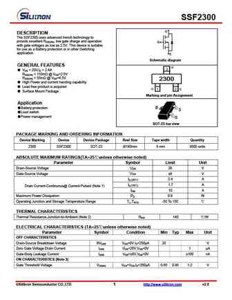
SSF2300 D DESCRIPTION The SSF2300 uses advanced trench technology to provide excellent RDS(ON), low gate charge and operation G with gate voltages as low as 2.5V. This device is suitable for use as a Battery protection or in other Switching application. S Schematic diagram GENERAL FEATURES VDS = 20V,ID = 2.4A RDS(ON) ... See More ⇒
ssf2300a.pdf
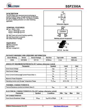
SSF2300A D DESCRIPTION The SSF2300A uses advanced trench technology to provide excellent RDS(ON), low gate charge and operation G with gate voltages as low as 2.5V. This device is suitable for use as a Battery protection or in other Switching application. S Schematic diagram GENERAL FEATURES VDS = 20V,ID = 4.5A RDS(ON) ... See More ⇒
ssf2300b.pdf
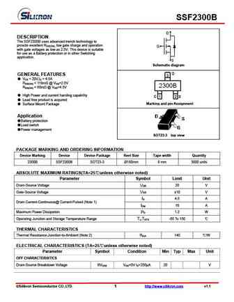
SSF2300B D DESCRIPTION The SSF2300B uses advanced trench technology to provide excellent R , low gate charge and operation DS(ON) G with gate voltages as low as 2.5V. This device is suitable for use as a Battery protection or in other Switching application. S Schematic diagram GENERAL FEATURES V = 20V,I = 4.5A DS D R ... See More ⇒
cs2300 sot-23.pdf
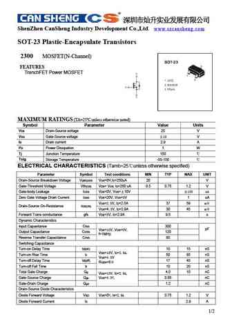
ShenZhen CanSheng Industry Development Co.,Ltd. www.szcansheng.com SOT-23 Plastic-Encapsulate Transistors 2300 MOSFET(N-Channel) FEATURES TrenchFET Power MOSFET MAXIMUM RATINGS (TA=25 unless otherwise noted) Symbol Parameter Value Units VDS Drain-Source voltage 20 V VGS Gate-Source voltage 10 V ID Drain current 2.9 A PD Power ... See More ⇒
brcs2300mc.pdf
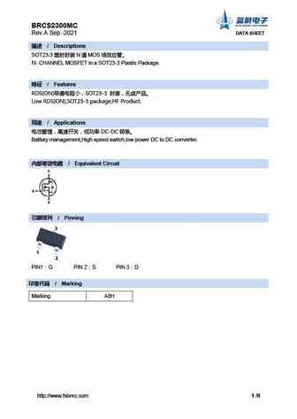
BRCS2300MC Rev.A Sep.-2021 DATA SHEET / Descriptions SOT23-3 N MOS N- CHANNEL MOSFET in a SOT23-3 Plastic Package. / Features RDS(ON) SOT23-3 Low RDS(ON),SOT23-3 package,HF Product. / Applications DC-DC Battery management,High spee... See More ⇒
brcs2300ma.pdf
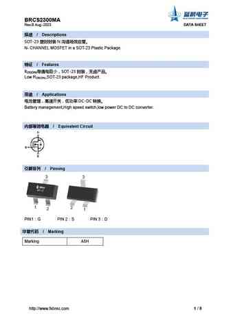
BRCS2300MA Rev.B Aug.-2023 DATA SHEET / Descriptions SOT-23 N N- CHANNEL MOSFET in a SOT-23 Plastic Package. / Features R SOT-23 DS(ON) Low R ,SOT-23 package,HF Product. DS(ON) / Applications DC-DC Battery management,High spee... See More ⇒
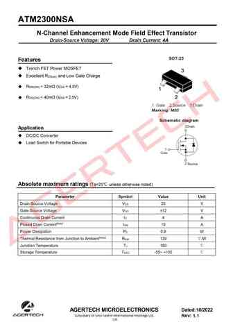
sm2300nsa.pdf
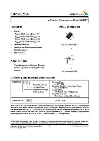
SM2300NSA N-Channel Enhancement Mode MOSFET Features Pin Description 20V/6A , D RDS(ON)=25m (max.) @ VGS=10V RDS(ON)=30m (max.) @ VGS=4.5V S RDS(ON)=40m (max.) @ VGS=2.5V G RDS(ON)=60m (max.) @ VGS=1.8V Reliable and Rugged Top View of SOT-23-3 Lead Free and Green Devices Available D (RoHS Compliant) ESD Protection G Applications Power Management in Notebook Computer... See More ⇒
sm2300nsan.pdf
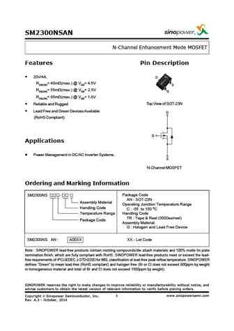
SM2300NSAN N-Channel Enhancement Mode MOSFET Features Pin Description 20V/4A, D RDS(ON)= 40m (max.) @ VGS= 4.5V S RDS(ON)= 55m (max.) @ VGS= 2.5V G RDS(ON)= 85m (max.) @ VGS= 1.8V Top View of SOT-23N Reliable and Rugged Lead Free and Green Devices Available D (RoHS Compliant) G Applications Power Management in DC/AC Inverter Systems. S N-Channel MOSFET ... See More ⇒
apm2300ca.pdf
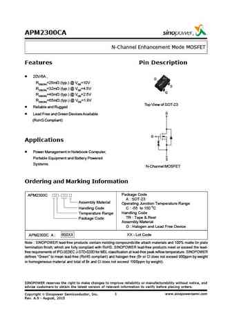
APM2300CA N-Channel Enhancement Mode MOSFET Features Pin Description 20V/6A , D RDS(ON)=25m (typ.) @ VGS=10V S RDS(ON)=32m (typ.) @ VGS=4.5V G RDS(ON)=40m (typ.) @ VGS=2.5V RDS(ON)=65m (typ.) @ VGS=1.8V Top View of SOT-23 Reliable and Rugged D Lead Free and Green Devices Available (RoHS Compliant) G Applications Power Management in Notebook Computer, Port... See More ⇒
dmn2300u.pdf
Product specification DMN2300U 20V N-CHANNEL ENHANCEMENT MODE MOSFET IN SOT23 Product Summary Features and Benefits On resistance ... See More ⇒
ki2300.pdf
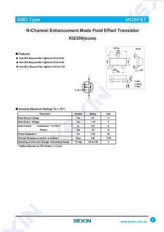
SMD Type IC SMD Type MOSFET N-Channel Enhancement Mode Field Effect Transistor KI2300(SI2300) SOT-23 Unit mm +0.1 2.9-0.1 +0.1 0.4-0.1 Features 3 VDS=20V,RDS(ON)=40m @VGS=4.5V,ID=5.0A VDS=20V,RDS(ON)=60m @VGS=2.5V,ID=4.0A VDS=20V,,RDS(ON)=75m @VGS=1.8V,ID=1.0A 12 +0.1 +0.05 0.95-0.1 0.1-0.01 +0.1 1.9-0.1 1.Base 1. Gate 2.Emitter 2. Source 3. Drain 3.collector Absolute... See More ⇒
si2300 ki2300.pdf
SMD Type IC SMD Type MOSFET N-Channel Enhancement MOSFET SI2300 (KI2300) SOT-23-3 Unit mm +0.2 2.9 -0.1 Features +0.1 0.4 -0.1 VDS=20V 3 ID=5.0A RDS(ON)=25m @VGS=4.5V,ID=5.0A RDS(ON)=35m @VGS=2.5V,ID=4.0A 1 2 +0.02 +0.1 0.15 -0.02 0.95 -0.1 RDS(ON)=55m @VGS=1.8V,ID=1.0A +0.1 1.9 -0.2 1. Gate 2. Source 3. Drain Absolute Maximum Ratings Ta = 25 Parameter Symbol Rating... See More ⇒
si2300-3.pdf
SMD Type IC SMD Type MOSFET N-Channel Enhancement MOSFET SI2300 (KI2300) SOT-23-3 Unit mm +0.2 2.9-0.1 Features +0.1 0.4 -0.1 VDS=20V,RDS(ON)=40m @VGS=4.5V,ID=5.0A 3 VDS=20V,RDS(ON)=60m @VGS=2.5V,ID=4.0A VDS=20V ,RDS(ON)=75m @VGS=1.8V,ID=1.0A 1 2 +0.02 +0.1 0.15 -0.02 0.95 -0.1 +0.1 1.9-0.2 1. Gate 2. Source 3. Drain Absolute Maximum Ratings Ta = 25 Parameter Symbol R... See More ⇒
khc2300.pdf
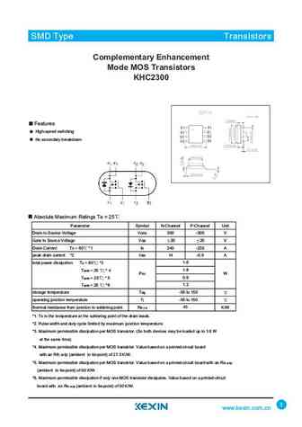
SMD Type IC SMD Type Transistors Complementary Enhancement Mode MOS Transistors KHC2300 Features High-speed switching No secondary breakdown. Absolute Maximum Ratings Ta = 25 Parameter Symbol N-Channel P-Channel Unit Drain to Source Voltage VDSS 300 -300 V Gate to Source Voltage VGS 20 20 V Drain Current Ts = 80 *1 ID 340 -235 A peak drain current *2 IDM 14 -0.9 A 1.6 total power... See More ⇒
si2300.pdf
SMD Type IC SMD Type MOSFET N-Channel Enhancement Mode Field Effect Transistor SI2300 (KI2300) SOT-23 Unit mm +0.1 2.9 -0.1 +0.1 0.4 -0.1 Features 3 VDS=20V,RDS(ON)=40m @VGS=4.5V,ID=5.0A VDS=20V,RDS(ON)=60m @VGS=2.5V,ID=4.0A VDS=20V,,RDS(ON)=75m @VGS=1.8V,ID=1.0A 1 2 +0.1 +0.05 0.95 -0.1 0.1 -0.01 +0.1 1.9 -0.1 1.Base 1. Gate 2.Emitter 2. Source 3. Drain 3.collector A... See More ⇒
am2300.pdf
AiT Semiconductor Inc. AM2300 www.ait-ic.com MOSFET 20V N-CHANNEL ENHANCEMENT MODE DESCRIPTION FEATURES The AM2300 is the N-Channel logic enhancement 20V/4.0A, R =26m (typ.)@V =4.5V DS(ON) GS mode power field effect transistor is produced using 20V/3.0A, R =31m (typ.)@V =2.5V DS(ON) GS high cell density. Advanced trench technology to 20V/2.0A, R =44m (typ.)@V =1.8... See More ⇒
gdssf2300.pdf
GDSSF2300 D DESCRIPTION The SSF2300 uses advanced trench technology to provide excellent RDS(ON), low gate charge and operation G with gate voltages as low as 2.5V. This device is suitable for use as a Battery protection or in other Switching application. S Schematic diagram GENERAL FEATURES VDS = 20V,ID = 2.4A RDS(ON) ... See More ⇒
kia2300.pdf
MOSFET TRANSISTORS 2300 KIA SEMICONDUCTORS 1. Features VDS=20V,RDS(ON)=30m @ VGS=10V,ID=6.0A VDS=20V,RDS(ON)=40m @ VGS=4.5V,ID=3.0A VDS=20V,RDS(ON)=55m @ VGS=2.5V,ID=2.0A 2. Pin information D Pin Function 1 Gate G 2 Source 3 Drain S 3. Maximum ratings (Ta=25 C) Characteristic Symbol Rating Unit Drain-source voltage VDS 20 V Gate-source volt... See More ⇒
mg12300wb-bn2mm.pdf
Power Module 1200V 300A IGBT Module RoHS MG12300WB-BN2MM Features IGBT3 CHIP(Trench+Field Free wheeling diodes Stop technology) with fast and soft reverse recovery Low saturation voltage and positive temperature Temperature sense coefficient included Fast switching and short tail current Applications AC motor control Photovoltaic/Fuel cell Mot... See More ⇒
mg12300d-ba1mm.pdf
Power Module 1200V 300A IGBT Module RoHS MG12300D-BA1MM Features Ultra low loss Positive temperature coefficient High ruggedness With fast free-wheeling High short circuit diodes capability Applications Inverter SMPS and UPS Converter Induction heating Welder Agency Approvals AGENCY AGENCY FILE NUMBER E71639 Module Characteristic... See More ⇒
mg12300d-bn3mm.pdf
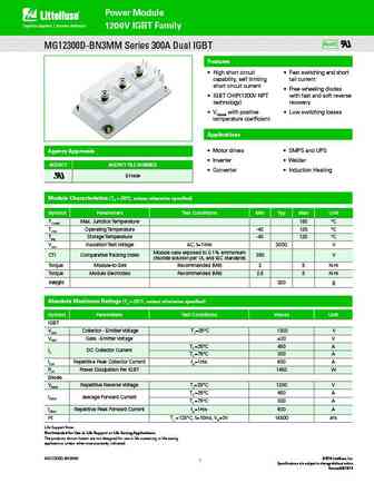
Power Module 1200V IGBT Family RoHS MG12300D-BN3MM Series 300A Dual IGBT Features High short circuit Fast switching and short capability, self limiting tail current short circuit current Free wheeling diodes IGBT CHIP(1200V NPT with fast and soft reverse technology) recovery VCE(sat) with positive Low switching losses temperature coefficient Applicat... See More ⇒
mg12300d-bn2mm.pdf
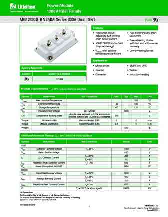
Power Module 1200V IGBT Family RoHS MG12300D-BN2MM Series 300A Dual IGBT Features High short circuit Fast switching and short capability, self limiting tail current short circuit current Free wheeling diodes IGBT3 CHIP(Trench+Field with fast and soft reverse Stop technology) recovery VCE(sat) with positive Low switching losses temperature coefficient ... See More ⇒
stn2300a.pdf
STN2300A 20V N-Channel Enhancement Mode MOSFET DESCRIPTION FEATURE The STN2300A is the N-Channel logic 20V/4.0A, RDS(ON) =22m (typ.)@VGS =4.5V enhancement mode power field effect transistor is 20V/3.0A, RDS(ON) =25m (typ.)@VGS =2.5V produced using high cell density. advanced trench 20V/2.0A, RDS(ON) =33m (typ.)@VGS =1.8V technology to provide excellent RD... See More ⇒
stn2300.pdf
STN2300 20V N-Channel Enhancement Mode MOSFET DESCRIPTION FEATURE The STN2300 is the N-Channel logic enhancement 20V/4.0A, RDS(ON) =26m (typ.)@VGS =4.5V mode power field effect transistor is produced using 20V/3.0A, RDS(ON) =35m (typ.)@VGS =2.5V high cell density. advanced trench technology to 20V/2.0A, RDS(ON) =50m (typ.)@VGS =1.8V provide excellent RDS... See More ⇒
sl2300.pdf
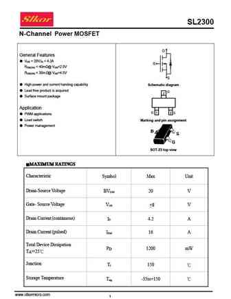
SL2300 N-Channel Power MOSFET D General Features VDS = 20V,ID = 4.2A G RDS(ON) ... See More ⇒
st2300.pdf
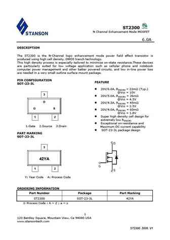
ST2300 N Channel Enhancement Mode MOSFET 6.0A DESCRIPTION The ST2300 is the N-Channel logic enhancement mode power field effect transistor is produced using high cell density, DMOS trench technology. This high density process is especially tailored to minimize on-state resistance.These devices are particularly suited for low voltage application such as cellular phone and noteboo... See More ⇒
st2300srg.pdf
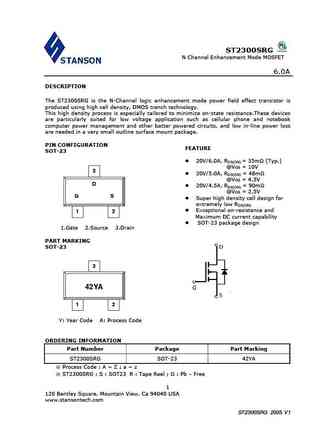
ST2300SRG N Channel Enhancement Mode MOSFET 6.0A DESCRIPTION The ST2300SRG is the N-Channel logic enhancement mode power field effect transistor is produced using high cell density, DMOS trench technology. This high density process is especially tailored to minimize on-state resistance.These devices are particularly suited for low voltage application such as cellular phone and n... See More ⇒
si2300a.pdf
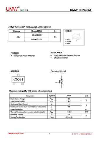
R UMW UMW SI2300A N-Channel 20-V(D-S) MOSFET UMW SI2300A ID SOT-23 V(BR)DSS RDS(on)MAX 25m @4.5V 20V 6 A 1. GATE 34.5m @2.5V 2. SOURCE 3. DRAIN APPLICATION FEA TURE Load Switch for Portable Devices TrenchFET Power MOSFET DC/DC Converter MARKING Equivalent Circuit C009T Maximum ratings (Ta=25 unless otherwise noted) Symbol Value Parameter Unit Dr... See More ⇒
as2300.pdf
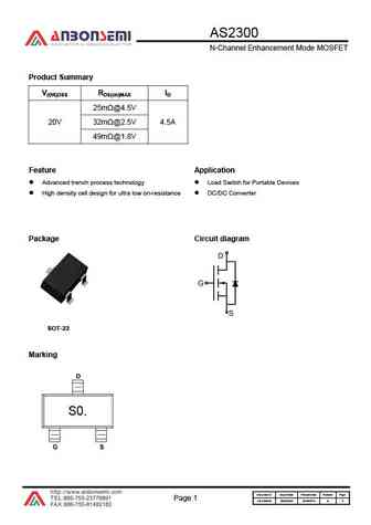
AS2300 N-Channel Enhancement Mode MOSFET Product Summary V(BR)DSS RDS(on)MAX ID 25m @4.5V 20V 32m @2.5V 4.5A 49m @1.8V Feature Application Advanced trench process technology Load Switch for Portable Devices High density cell design for ultra low on-resistance DC/DC Converter Package Circuit diagram SOT-23 Marking S0. Document ID Issued Date Revised Date Revision... See More ⇒
asdm2300za.pdf
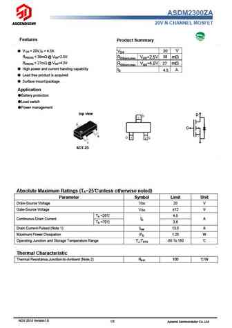
ASDM2300ZA 20V N-CHANNEL MOSFET Features Product Summary V = 20V,ID = 4.5A 20 V DS VDS RDS(ON) ... See More ⇒
bm2300.pdf
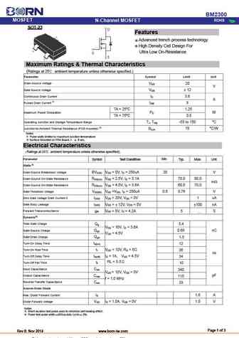
BM2300 MOSFET ROHS N-Channel MOSFET SOT-23 - Features Advanced trench process technology High Density Cell Design For Ultra Low On-Resistance Maximum Ratings & Thermal Characteristics (Ratings at 25 ambient temperature unless otherwise specified.) Parameter Symbol Limit Unit Drain-Source Voltage V 20 DS V Gate-Source Voltage V 12 GS Continuous Drain Cur... See More ⇒
en2300.pdf
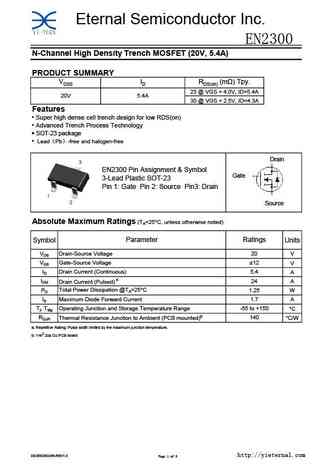
Eternal Semiconductor Inc. EN2300 N-Channel High Density Trench MOSFET (20V, 5.4A) PRODUCT SUMMARY VDSS ID RDS(on) (m ) Tpy. 23 @ VGS = 4.0V, ID=5.4A 20V 5.4A 30 @ VGS = 2.5V, ID=4.3A Features Super high dense cell trench design for low RDS(on) Advanced Trench Process Technology SOT-23 package Lead Pb -free and halogen-free Drain EN2300 Pin Assignment & Symb... See More ⇒
si2300.pdf
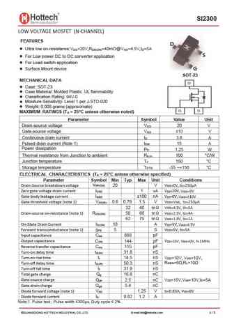
SI2300 LOW VOLTAGE MOSFET (N-CHANNEL) FEATURES Ultra low on-resistance V =20V,R =40m @V =4.5V,I =5A DS DS(ON) GS D For Low power DC to DC converter application For Load switch application Surface Mount device SOT-23 MECHANICAL DATA Case SOT-23 Case Material Molded Plastic. UL flammability Classification Rating 94V-0 Moisture Sensitivity Level 1 ... See More ⇒
hss2300a.pdf
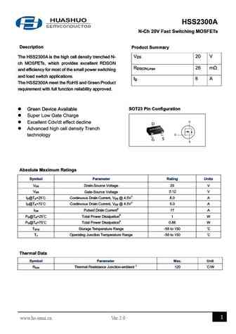
HSS2300A N-Ch 20V Fast Switching MOSFETs Description Product Summary VDS 20 V The HSS2300A is the high cell density trenched N- ch MOSFETs, which provides excellent RDSON RDS(ON),max 26 m and efficiency for most of the small power switching and load switch applications. ID 6 A The HSS2300A meet the RoHS and Green Product requirement with full function reliability approved... See More ⇒
hx2300a.pdf
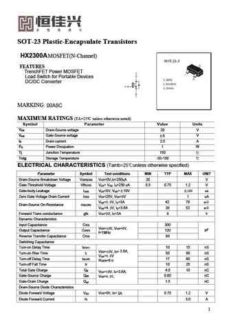
SOT-23 Plastic-Encapsulate Transistors HX2300AMOSFET(N-Channel) FEATURES TrenchFET Power MOSFET Load Switch for Portable Devices DC/DC Converter MARKING 00A8C MAXIMUM RATINGS (TA=25 unless otherwise noted) Symbol Parameter Value Units V Drain-Source voltage 20 V DS V Gate-Source voltage 8 V GS I Drain current 2.5 A D P Power Dissipation 1 W D Tj Junction Temperature 150 ... See More ⇒
hx2300.pdf

SOT-23-3 Plastic-Encapsulate Transistors HX2300MOSFET(N-Channel) FEATURES TrenchFET Power MOSFET Load Switch for Portable Devices DC/DC Converter MARKING 00A8C MAXIMUM RATINGS (TA=25 unless otherwise noted) Symbol Parameter Value Units VDS Drain-Source voltage 20 V VGS Gate-Source voltage 8 V ID Drain current 3.6 A PD Power Dissipation 1 W Tj Junction Temperature 150 Ts... See More ⇒
jst2300.pdf
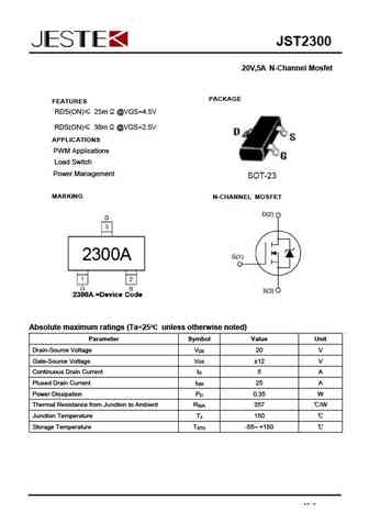
JST2300 20V,5A N-Channel Mosfet PACKAGE FEATURES RDS(ON) 25m @VGS=4.5V RDS(ON) 38m @VGS=2.5V APPLICATIONS PWM Applications Load Switch Power Management MARKING N-CHANNEL MOSFET Absolute maximum ratings (Ta=25 unless otherwise noted) Parameter Symbol Value Unit Drain-Source Voltage V 20 V DS Gate-Source Voltage V 12 V GS Continuous Drain Current I 5 A D Pl... See More ⇒
si2300.pdf
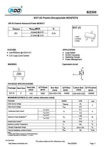
SI2300 SOT-23 Plastic-Encapsulate MOSFETS 20V N-Channel Advanced Power MOSFET SOT-23 ID V(BR)DSS RDS(on)MAX 3 19.4m @ 4.5V 20V 6.2A 21.5m @ 3.3V 1. GATE 2. SOURCE 1 3. DRAIN 2 FEATURE APPLICATION Low RDS(on) @VGS=4.5V Load Switch DC/DC Converter 3.3V Logic Level Control Switching Circuits Power Management MARKING Equivalent circuit D 2300 G S... See More ⇒
si2300.pdf
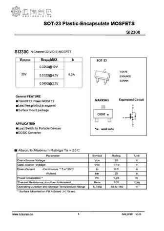
SOT-23 Plastic-Encapsulate MOSFETS SMD Type IC SMD Type MOSFET SI2300 N-Channel 20-V(D-S) MOSFET SI2300 V(BR)DSS RDS(on)MAX ID SOT-23 0.025 @10V 3 1.GATE 20V 6.0A 0.032 @4.5V 2.SOURCE 3.DRAIN 1 0.040 @2.5V 2 General FEATURE Equivalent Circuit MARKING TrenchFET Power MOSFET Lead free product is acquired Surface mount package C009T w APPLICATION Load Switc... See More ⇒
pjm2300nsa-l.pdf
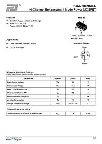
PJM2300NSA-L N-Channel Enhancement Mode Power MOSFET Features SOT-23 Excellent R and Low Gate Charge DS(ON) VDS= 20V I = 5.5A D R ... See More ⇒
pjm2300nsa.pdf
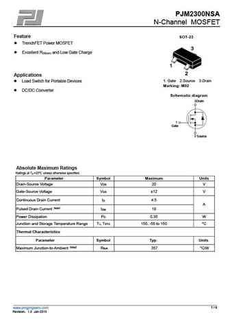
PJM2300NSA N-Channel MOSFET Feature SOT-23 TrenchFET Power MOSFET Excellent R and Low Gate Charge DS(on) Applications 1. Gate 2.Source 3.Drain Load Switch for Portable Devices Marking M02 DC/DC Converter Schematic diagram 3Drain 1 Gate 2 Source Absolute Maximum Ratings Ratings at TA =25 unless otherwise specified. Parameter Symbol Maximum Units ... See More ⇒
si2300.pdf
SI2300 20V N-Channel Enhancement Mode MOSFET VDS= 20V RDS(ON), Vgs@ 4.5V, Ids@ 3.6A 70m RDS(ON), Vgs@ 2.5V, Ids@ 3.1A 80m Features Advanced trench process technology High Density Cell Design For Ultra Low On-Resistance High Power and Current handing capability Ideal for Li ion battery pack applications Package Dimensions D SOT-23 G S Millimeter Millimeter R... See More ⇒
wtm2300.pdf
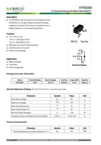
WTM2300 N-Channel Enhancement Mode Power MOSFET Description The WTM2300 uses advanced trench technology to provide excellent R , low gate charge and operation with gate DS(ON) voltages as low as 2.5V. This device is suitable for use as a battery protection or in other switching application. Features V DS = 20V, lD = 6A R ... See More ⇒
si2300.pdf
SI2300 N-Channel 20-V(D-S) MOSFET ID SOT-23-3L V(BR)DSS RDS(on)MAX 40m @4.5V 20V 3A 1. GATE 75 m @2.5V 2. SOURCE 3. DRAIN FEA TURE APPLICATION Load Switch for Portable Devices TrenchFET Power MOSFET DC/DC Converter MARKING Equivalent Circuit 2300 Maximum ratings (Ta=25 unless otherwise noted) Symbol Value Parameter Unit Drain-Source Volta... See More ⇒
si2300.pdf
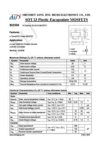
SHENZHEN LONG JING MICRO-ELECTRONICS CO., LTD. SOT-23 Plastic-Encapsulate MOSFETS SI2300 N-Channel 20V(D-S) MOSFET Features TrenchFET Power MOSFET Application Load Switch for Portable Devices DC/DC Converter 1. GATE Marking AOSHB 2. SOURCE 3. DRAIN Maximum Ratings (T =25 C unless otherwise noted) a Symbol Parameter Value Unit V Drain-source voltage 20 V DS... See More ⇒
tf2300.pdf
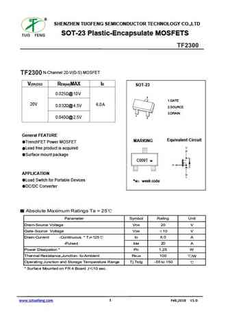
SHENZHEN TUOFENG SEMICONDUCTOR TECHNOLOGY CO.,LTD SOT-23 Plastic-Encapsulate MOSFETS SMD Type IC SMD Type MOSFET TF2300 N-Channel 20-V(D-S) MOSFET TF2300 V(BR)DSS RDS(on)MAX ID SOT-23 0.025 @10V 3 1.GATE 20V 6.0A 0.032 @4.5V 2.SOURCE 3.DRAIN 1 0.040 @2.5V 2 General FEATURE Equivalent Circuit MARKING TrenchFET Power MOSFET Lead free product is acquired Surface... See More ⇒
si2300.pdf
SI2300 SI2301 Features VDS=20V,RDS(ON)=40m @VGS=4.5V,ID=5.0A VDS=20V,RDS(ON)=60m @VGS=2.5V,ID=4.0A VDS=20V,,RDS(ON)=75m @VGS=1.8V,ID=1.0A Equivalent Circuit MARKING 2300 3400 R 3400 1.GATE 2.SOURCE 3.DRAIN Absolute Maximum Ratings Ta = 25 Parameter Symbol Rating Unit Drain-Source Voltage VDS 20 V Gate-Source V... See More ⇒
wst2300.pdf
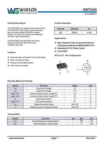
WST2300 N-Ch MOSFET General Description Product Summery The WST2300 is the highest performance trench BVDSS RDSON ID N-Ch MOSFET with extreme high cell density , which provide excellent RDSON and gate 20V 50m 4.4A charge for most of the small power switching and load switch applications. Applications The WST2300 meet the RoHS and Green Product requirement with full funct... See More ⇒
wst2300a.pdf
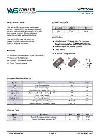
WST2300A N-Ch MOSFET General Description Product Summery The WST2300A is the highest performance BVDSS RDSON ID trench N-Ch MOSFET with extreme high cell density , which provide excellent RDSON and 20V 60m 3.0A gate charge for most of the small power switching and load switch applications. Applications The WST2300A meet the RoHS and Green Product requirement with full ... See More ⇒
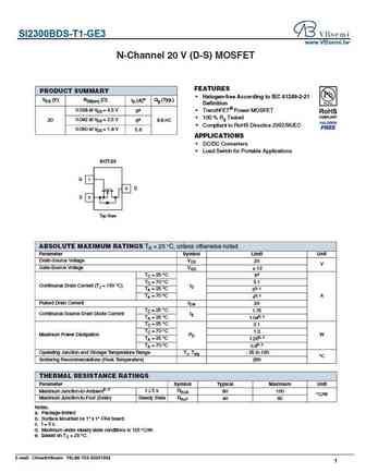
si2300ds-t1-ge3.pdf

SI2300DS-T1-GE3 www.VBsemi.tw N-Channel 20 V (D-S) MOSFET FEATURES PRODUCT SUMMARY Halogen-free According to IEC 61249-2-21 VDS (V) RDS(on) ( ) ID (A)e Qg (Typ.) Definition 0.028 at VGS = 4.5 V TrenchFET Power MOSFET 6a 100 % Rg Tested 20 0.042 at VGS = 2.5 V 6a 8.8 nC Compliant to RoHS Directive 2002/95/EC 0.050 at VGS = 1.8 V 5.6 APPLICATIONS DC/D... See More ⇒
sm2300nsac.pdf
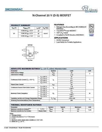
SM2300NSAC www.VBsemi.tw N-Channel 20 V (D-S) MOSFET FEATURES PRODUCT SUMMARY Halogen-free According to IEC 61249-2-21 VDS (V) RDS(on) ( ) ID (A)e Qg (Typ.) Definition 0.028 at VGS = 4.5 V TrenchFET Power MOSFET 6a 100 % Rg Tested 20 0.042 at VGS = 2.5 V 6a 8.8 nC Compliant to RoHS Directive 2002/95/EC 0.050 at VGS = 1.8 V 5.6 APPLICATIONS DC/D... See More ⇒
apm2300cac.pdf
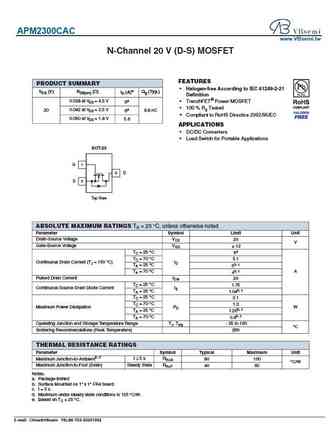
APM2300CAC www.VBsemi.tw N-Channel 20 V (D-S) MOSFET FEATURES PRODUCT SUMMARY Halogen-free According to IEC 61249-2-21 VDS (V) RDS(on) ( ) ID (A)e Qg (Typ.) Definition 0.028 at VGS = 4.5 V TrenchFET Power MOSFET 6a 100 % Rg Tested 20 0.042 at VGS = 2.5 V 6a 8.8 nC Compliant to RoHS Directive 2002/95/EC 0.050 at VGS = 1.8 V 5.6 APPLICATIONS DC/D... See More ⇒
si2300bds-t1-ge3.pdf
SI2300BDS-T1-GE3 www.VBsemi.tw N-Channel 20 V (D-S) MOSFET FEATURES PRODUCT SUMMARY Halogen-free According to IEC 61249-2-21 VDS (V) RDS(on) ( ) ID (A)e Qg (Typ.) Definition 0.028 at VGS = 4.5 V TrenchFET Power MOSFET 6a 100 % Rg Tested 20 0.042 at VGS = 2.5 V 6a 8.8 nC Compliant to RoHS Directive 2002/95/EC 0.050 at VGS = 1.8 V 5.6 APPLICATIONS DC/... See More ⇒
ap2300gn.pdf
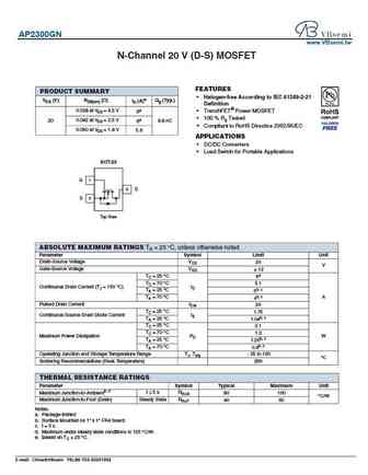
AP2300GN www.VBsemi.tw N-Channel 20 V (D-S) MOSFET FEATURES PRODUCT SUMMARY Halogen-free According to IEC 61249-2-21 VDS (V) RDS(on) ( ) ID (A)e Qg (Typ.) Definition 0.028 at VGS = 4.5 V TrenchFET Power MOSFET 6a 100 % Rg Tested 20 0.042 at VGS = 2.5 V 6a 8.8 nC Compliant to RoHS Directive 2002/95/EC 0.050 at VGS = 1.8 V 5.6 APPLICATIONS DC/DC Conve... See More ⇒
hm2300.pdf

HM2300 www.VBsemi.tw N-Channel 20 V (D-S) MOSFET FEATURES PRODUCT SUMMARY Halogen-free According to IEC 61249-2-21 VDS (V) RDS(on) ( ) ID (A)e Qg (Typ.) Definition 0.028 at VGS = 4.5 V TrenchFET Power MOSFET 6a 100 % Rg Tested 20 0.042 at VGS = 2.5 V 6a 8.8 nC Compliant to RoHS Directive 2002/95/EC 0.050 at VGS = 1.8 V 5.6 APPLICATIONS DC/DC Convert... See More ⇒
st2300s23rg.pdf
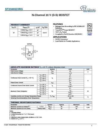
ST2300S23RG www.VBsemi.tw N-Channel 20 V (D-S) MOSFET FEATURES PRODUCT SUMMARY Halogen-free According to IEC 61249-2-21 VDS (V) RDS(on) ( ) ID (A)e Qg (Typ.) Definition 0.028 at VGS = 4.5 V TrenchFET Power MOSFET 6a 100 % Rg Tested 20 0.042 at VGS = 2.5 V 6a 8.8 nC Compliant to RoHS Directive 2002/95/EC 0.050 at VGS = 1.8 V 5.6 APPLICATIONS DC/... See More ⇒
mt2300actr.pdf
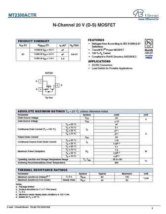
MT2300ACTR www.VBsemi.tw N-Channel 20 V (D-S) MOSFET FEATURES PRODUCT SUMMARY Halogen-free According to IEC 61249-2-21 VDS (V) RDS(on) ( ) ID (A)e Qg (Typ.) Definition 0.028 at VGS = 4.5 V TrenchFET Power MOSFET 6a 100 % Rg Tested 20 0.042 at VGS = 2.5 V 6a 8.8 nC Compliant to RoHS Directive 2002/95/EC 0.050 at VGS = 1.8 V 5.6 APPLICATIONS DC/DC Con... See More ⇒
yjl2300a.pdf
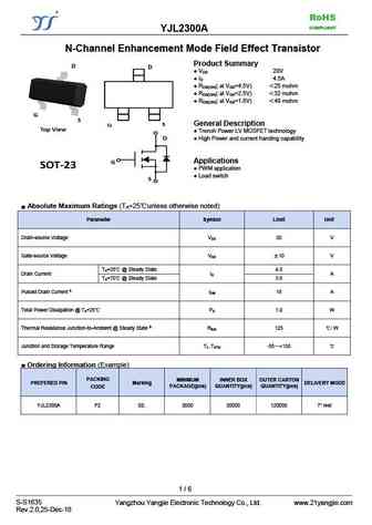
RoHS COMPLIANT YJL2300A N-Channel Enhancement Mode Field Effect Transistor Product Summary V 20V DS I 4.5A D R ( at V =4.5V) 25 mohm DS(ON) GS R ( at V =2.5V) 32 mohm DS(ON) GS R ( at V =1.8V) 49 mohm DS(ON) GS General Description Trench Power LV MOSFET technology High Power and current handing capability Applications PW... See More ⇒
hm2300d.pdf

HM2300D N-Channel Enhancement Mode Power MOSFET Description D The HM2300D uses advanced trench technology to provide excellent RDS(ON), low gate charge and operation with gate G voltages as low as 2.5V. This device is suitable for use as a battery protection or in other switching application. S Schematic diagram General Features VDS = 20V,ID = 6.0A RDS(ON) ... See More ⇒
hm2300b.pdf
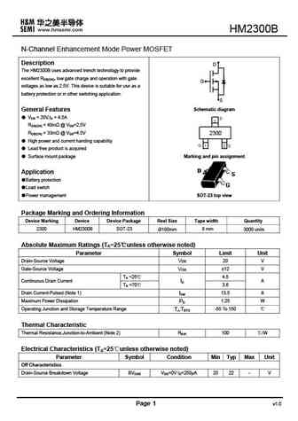
HM2300B N-Channel Enhancement Mode Power MOSFET Description D The HM2300B uses advanced trench technology to provide excellent RDS(ON), low gate charge and operation with gate G voltages as low as 2.5V. This device is suitable for use as a battery protection or in other switching application. S Schematic diagram General Features VDS = 20V,ID = 4.5A RDS(ON) ... See More ⇒
hm2300pr.pdf
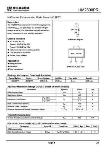
HM2300PR N-Channel Enhancement Mode Power MOSFET Description D The HM2300PR uses advanced trench technology to provide excellent RDS(ON), low gate charge and operation with gate G voltages as low as 2.5V. This device is suitable for use as a battery protection or in other switching application. S General Features Schematic diagram VDS = 20V,ID = 5.5A RDS(ON) ... See More ⇒
hm2300c.pdf

HM2300C N-Channel Enhancement Mode Power MOSFET Description D The HM2300C uses advanced trench technology to provide excellent RDS(ON), low gate charge and operation with gate G voltages as low as 2.5V. This device is suitable for use as a battery protection or in other switching application. S Schematic diagram General Features VDS = 20V,ID = 6.0A RDS(ON) ... See More ⇒
hm2300dr.pdf
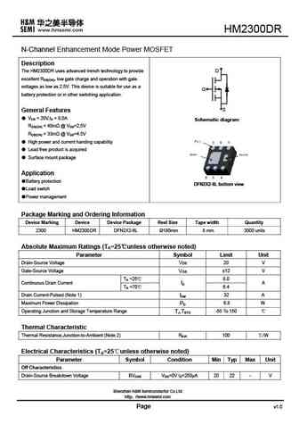
HM2300DR N-Channel Enhancement Mode Power MOSFET Description The HM2300DR uses advanced trench technology to provide D excellent RDS(ON), low gate charge and operation with gate voltages as low as 2.5V. This device is suitable for use as a G battery protection or in other switching application. S General Features VDS = 20V,ID = 8.0A Schematic diagram RDS(ON) ... See More ⇒
hm2300.pdf
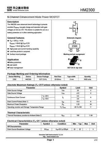
HM2300 N-Channel Enhancement Mode Power MOSFET Description D The HM2300 uses advanced trench technology to provide excellent RDS(ON), low gate charge and operation with gate G voltages as low as 2.5V. This device is suitable for use as a battery protection or in other switching application. S Schematic diagram General Features VDS = 20V,ID = 4.5A RDS(ON) ... See More ⇒
2sd2300.pdf
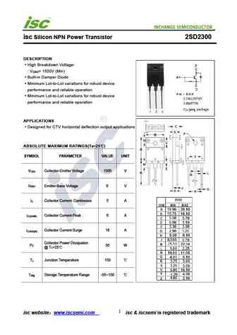
isc Silicon NPN Power Transistor 2SD2300 DESCRIPTION High Breakdown Voltage- V = 1500V (Min) CBO Built-in Damper Diode Minimum Lot-to-Lot variations for robust device performance and reliable operation Minimum Lot-to-Lot variations for robust device performance and reliable operation APPLICATIONS Designed for CTV horizontal deflection output applications. ABSOLUTE MAXIMU... See More ⇒
ap2300mi.pdf
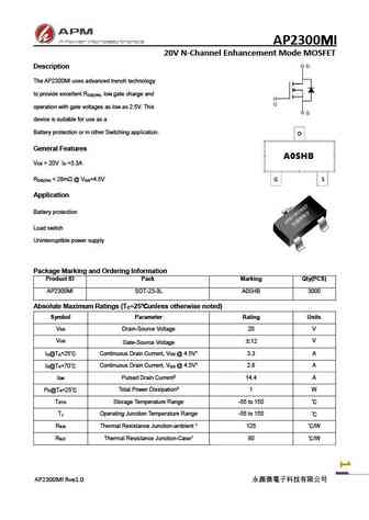
AP2300MI 20V N-Channel Enhancement Mode MOSFET Description The AP2300MI uses advanced trench technology to provide excellent R , low gate charge and DS(ON) operation with gate voltages as low as 2.5V. This device is suitable for use as a Battery protection or in other Switching application. General Features V = 20V I =3.3A DS D R ... See More ⇒
ap2300ai.pdf
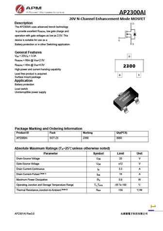
AP2300AI 20V N-Channel Enhancement Mode MOSFET Description The AP2300AI uses advanced trench technology to provide excellent R , low gate charge and DS(ON) operation with gate voltages as low as 2.5V. This device is suitable for use as a Battery protection or in other Switching application. General Features V = 20V,I = 3.3A DS D R ... See More ⇒
Detailed specifications: SSS2N60, SSS5N60, SSS7N60, SSS8N60, 1002, 1115, 1515, G1601, 3401, 2301, 2302, 3035, 3400, 3401, 3415, 6616, 6703
Keywords - 2300 MOSFET specs
2300 cross reference
2300 equivalent finder
2300 pdf lookup
2300 substitution
2300 replacement
Learn how to find the right MOSFET substitute. A guide to cross-reference, check specs and replace MOSFETs in your circuits.
MOSFET Parameters. How They Affect Each Other
History: 19MT050XF | 18N50A
🌐 : EN ES РУ

LIST
Last Update
MOSFET: CEZC2P07 | CEZ2R05 | CEU3133 | CES2361 | CES2312A | CEP100N10L | CEM3425 | CEM3139 | CEM3133 | CEM3115
Popular searches
mp10b transistor | bc182b | 2n3054 transistor equivalent | 2n554 | 2sa1011 | 2sa1283 | 2sb646 | 2sc1885 datasheet