2302 Specs and Replacement
Type Designator: 2302
Type of Transistor: MOSFET
Type of Control Channel: N-Channel
Absolute Maximum Ratings
Pd ⓘ - Maximum Power Dissipation: 1 W
|Vds|ⓘ - Maximum Drain-Source Voltage: 20 V
|Vgs|ⓘ - Maximum Gate-Source Voltage: 10 V
|Id| ⓘ - Maximum Drain Current: 2.9 A
Tj ⓘ - Maximum Junction Temperature: 150 °C
Electrical Characteristics
tr ⓘ - Rise Time: 50 nS
Cossⓘ - Output Capacitance: 120 pF
RDSonⓘ - Maximum Drain-Source On-State Resistance: 0.045 Ohm
Package: SOT23
2302 substitution
- MOSFET ⓘ Cross-Reference Search
2302 datasheet
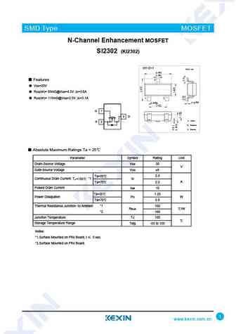
si2302ds.pdf
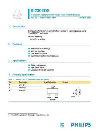
SI2302DS N-channel enhancement mode field-effect transistor Rev. 02 20 November 2001 Product data M3D088 1. Description N-channel enhancement mode field-effect transistor in a plastic package using TrenchMOS 1 technology. Product availability SI2302DS in SOT23. 2. Features TrenchMOS technology Very fast switching Logic level compatible Subminiature surface mount packa... See More ⇒
msc82302.pdf
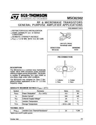
MSC82302 RF & MICROWAVE TRANSISTORS GENERAL PURPOSE AMPLIFIER APPLICATIONS PRELIMINARY DATA .REFRACTORY/GOLD METALLIZATION .VSWR CAPABILITY 20 1 @ RATED CONDITIONS .HERMETIC STRIPAC PACKAGE .P 1.8 W MIN. WITH 10.0 dB GAIN OUT = .250 2LFL (S010) hermetically sealed ORDER CODE BRANDING MSC82302 82302 PIN CONNECTION DESCRIPTION The MSC82302 is a common base hermetically sealed ... See More ⇒
rn2301 rn2302 rn2303 rn2304 rn2305 rn2306.pdf
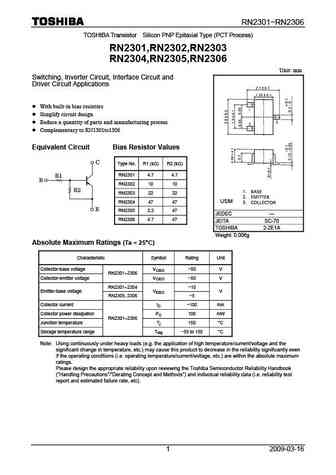
RN2301 RN2306 TOSHIBA Transistor Silicon PNP Epitaxial Type (PCT Process) RN2301,RN2302,RN2303 RN2304,RN2305,RN2306 Unit mm Switching, Inverter Circuit, Interface Circuit and Driver Circuit Applications With built-in bias resistors Simplify circuit design Reduce a quantity of parts and manufacturing process Complementary to RN1301to1306 Equivalent Circuit Bias Resi... See More ⇒
si2302cds.pdf
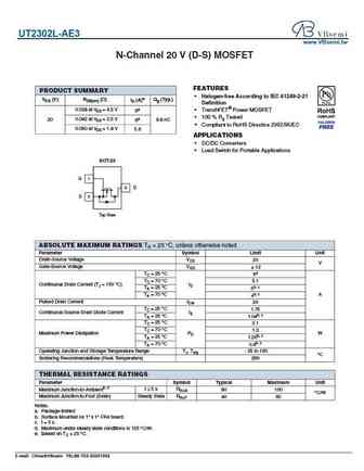
Si2302CDS Vishay Siliconix N-Channel 20 V (D-S) MOSFET FEATURES PRODUCT SUMMARY TrenchFET Power MOSFET VDS (V) RDS(on) ( )ID (A) Qg (Typ.) Material categorization 0.057 at VGS = 4.5 V 2.9 For definitions of compliance please see 20 3.5 0.075 at VGS = 2.5 V www.vishay.com/doc?99912 2.6 APPLICATIONS Load Switching for Portable Devices DC/DC Converter TO... See More ⇒
si2302dds.pdf
Si2302DDS Vishay Siliconix N-Channel 20 V (D-S) MOSFET FEATURES PRODUCT SUMMARY Halogen-free According to IEC 61249-2-21 VDS (V) RDS(on) ( ) Max. ID (A) Qg (Typ.) Definition 0.057 at VGS = 4.5 V 2.9 TrenchFET Power MOSFET 20 3.5 0.075 at VGS = 2.5 V 100 % Rg Tested 2.6 Compliant to RoHS Directive 2002/95/EC APPLICATIONS Load Switching for Portable Dev... See More ⇒
si2302ds.pdf
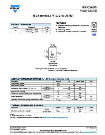
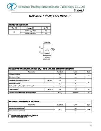
Si2302DS Vishay Siliconix N-Channel 1.25-W, 2.5-V MOSFET PRODUCT SUMMARY VDS (V) rDS(on) (W) ID (A) 0.085 @ VGS = 4.5 V 2.8 20 20 0.115 @ VGS = 2.5 V 2.4 TO-236 (SOT-23) G 1 3 D S 2 Top View Si2302DS (A2)* *Marking Code ABSOLUTE MAXIMUM RATINGS (TA = 25_C UNLESS OTHERWISE NOTED) Parameter Symbol Limit Unit Drain-Source Voltage VDS 20 V V Gate-Source Voltage VGS "8 TA= 25_... See More ⇒
si2302ad.pdf
Si2302ADS Vishay Siliconix N-Channel 2.5-V (G-S) MOSFET FEATURES PRODUCT SUMMARY Halogen-free According to IEC 61249-2-21 VDS (V) RDS(on) ( )ID (A) Definition 0.060 at VGS = 4.5 V 2.4 Compliant to RoHS Directive 2002/95/EC 20 0.115 at VGS = 2.5 V 2.0 TO-236 (SOT-23) G 1 3 D S 2 Top View Si2302ADS (2A)* * Marking Code Ordering Information Si2302ADS-T1-E3 (... See More ⇒
si2302cd.pdf
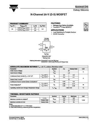
Si2302CDS Vishay Siliconix N-Channel 20-V (D-S) MOSFET FEATURES PRODUCT SUMMARY Halogen-free Option Available VDS (V) RDS(on) ( )ID (A) Qg (Typ.) TrenchFET Power MOSFET 0.057 at VGS = 4.5 V 2.9 20 3.5 RoHS 0.075 at VGS = 2.5 V APPLICATIONS 2.6 COMPLIANT Load Switching for Portable Devices DC/DC Converter TO-236 (SOT-23) G 1 3 D S 2 Top View Si2302... See More ⇒
si2302-tp.pdf
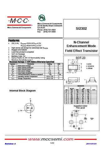
MCC Micro Commercial Components TM 20736 Marilla Street Chatsworth Micro Commercial Components CA 91311 SI2302 Phone (818) 701-4933 Fax (818) 701-4939 Features N-Channel 20V,3.0A, RDS(ON)=55m @VGS=4.5V RDS(ON)=82m @VGS=2.5V Enhancement Mode High dense cell design for extremely low RDS(ON) Rugged and reliable Field Effect Transistor Lead free product is acqu... See More ⇒
si2302ads-t1 si2302ads.pdf
Si2302ADS Vishay Siliconix N-Channel 2.5-V (G-S) MOSFET FEATURES PRODUCT SUMMARY Halogen-free According to IEC 61249-2-21 VDS (V) RDS(on) ( )ID (A) Definition 0.060 at VGS = 4.5 V 2.4 100 % Rg Tested 20 Compliant to RoHS Directive 2002/95/EC 0.115 at VGS = 2.5 V 2.0 TO-236 (SOT-23) G 1 3 D S 2 Top View Si2302ADS (2A)* * Marking Code Ordering Informatio... See More ⇒
dmg2302uq.pdf
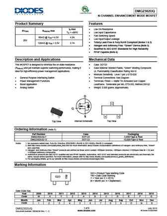
DMG2302UQ N-CHANNEL ENHANCEMENT MODE MOSFET Product Summary Features Low On-Resistance ID max BVDSS RDS(ON) max TA = +25 C Low Input Capacitance Fast Switching Speed 90m @ VGS = 4.5V 4.2A Low Input/Output Leakage 20V Totally Lead-Free & Fully RoHS Compliant (Notes 1 & 2) 120m @ VGS = 2.5V 2.7A Halogen and Antimony Free. Green Device... See More ⇒
dmg2302uk.pdf
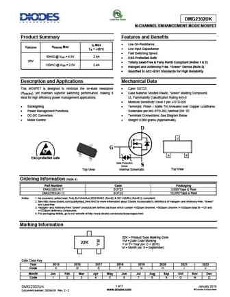
DMG2302UK N-CHANNEL ENHANCEMENT MODE MOSFET Product Summary Features and Benefits Low On-Resistance ID Max V(BR)DSS RDS(ON) Max Low Input Capacitance TA = +25 C Fast Switching Speed 90m @ VGS = 4.5V 2.8A ESD Protected Gate 20V Totally Lead-Free & Fully RoHS Compliant (Notes 1 & 2) 120m @ VGS = 2.5V 2.4A Halogen and Antimony Free. Gre... See More ⇒
dmg2302u.pdf
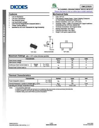
DMG2302U N-CHANNEL ENHANCEMENT MODE MOSFET Please click here to visit our online spice models database. Features Mechanical Data Low On-Resistance Case SOT-23 Low Input Capacitance Case Material Molded Plastic, Green Molding Compound. UL Flammability Classification Rating 94V-0 Fast Switching Speed Moisture Sensitivity Level 1 per J-STD-020D L... See More ⇒
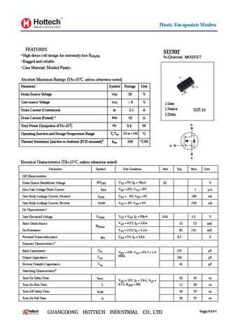
si2302.pdf

MCC Micro Commercial Components TM 20736 Marilla Street Chatsworth Micro Commercial Components CA 91311 SI2302 Phone (818) 701-4933 Fax (818) 701-4939 Features N-Channel 20V,3.0A, RDS(ON)=55m @VGS=4.5V RDS(ON)=82m @VGS=2.5V Enhancement Mode High dense cell design for extremely low RDS(ON) Rugged and reliable Field Effect Transistor Lead free product is acqu... See More ⇒
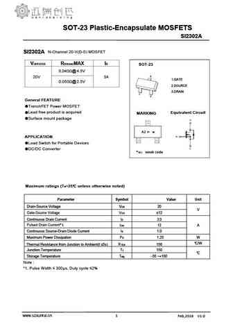
si2302a.pdf
SI2302A Features Rugged and Reliable Lead Free Product is Acquired High Dense Cell Design for Extremely Low RDS(ON) N-Channel Epoxy Meets UL 94 V-0 Flammability Rating Moisture Sensitivity Level 1 Enhancement Mode Halogen Free Available Upon Request by Adding Suffix "-HF" Lead Free Finish/RoHS Compliant ("P" Suffix Designates RoHS Field Effect Transistor ... See More ⇒
ut2302.pdf
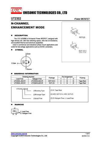
UNISONIC TECHNOLOGIES CO., LTD UT2302 Power MOSFET N-CHANNEL ENHANCEMENT MODE DESCRIPTION The UTC UT2302 is N-channel Power MOSFET, designed with high density cell, with fast switching speed, ultra low on-resistance, and excellent thermal and electrical capabilities. Used in commercial and industrial surface mount applications and suited for low voltage applications such as ... See More ⇒
ut2302g-ae2-r ut2302g-ae3-r.pdf
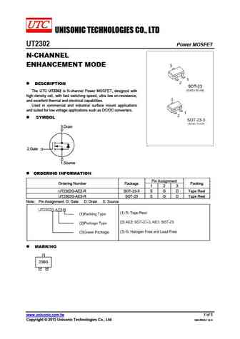
UNISONIC TECHNOLOGIES CO., LTD UT2302 Power MOSFET N-CHANNEL ENHANCEMENT MODE DESCRIPTION The UTC UT2302 is N-channel Power MOSFET, designed with high density cell, with fast switching speed, ultra low on-resistance, and excellent thermal and electrical capabilities. Used in commercial and industrial surface mount applications and suited for low voltage applications such a... See More ⇒
smg2302.pdf
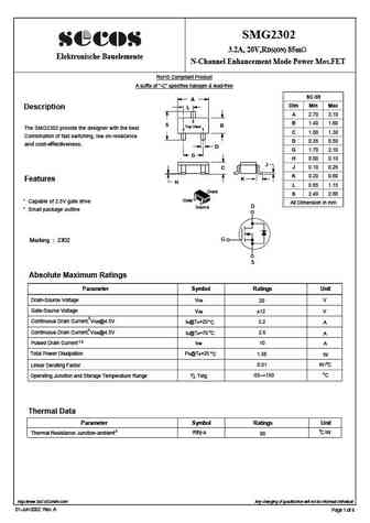
SMG2302 3.2A, 20V,RDS(ON) 85m Elektronische Bauelemente N-Channel Enhancement Mode Power Mos.FET RoHS Compliant Product A suffix of "-C" specifies halogen & lead-free SC-59 A Dim Min Max Description L A 2.70 3.10 3 B 1.40 1.60 S B Top View The SMG2302 provide the designer with the best 2 1 C 1.00 1.30 Combination of fast switching, low on-resistance D 0.35 0.50 and ... See More ⇒
smg2302n.pdf
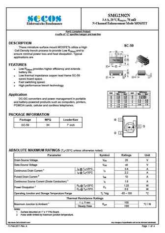
SMG2302N 3.4 A, 20 V, RDS(ON) 76 m N-Channel Enhancement Mode MOSFET Elektronische Bauelemente RoHS Compliant Product A suffix of -C specifies halogen and lead-free DESCRIPTION SC-59 These miniature surface mount MOSFETs utilize a High Cell Density trench process to provide Low RDS(on) and to A L ensure minimal power loss and heat dissipation. Typical 3 3 app... See More ⇒
tsm2302 a07.pdf
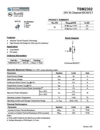
TSM2302 20V N-Channel MOSFET PRODUCT SUMMARY SOT-23 Pin Definition VDS (V) RDS(on)(m ) ID (A) 1. Gate 2. Source 65 @ VGS = 4.5V 2.8 3. Drain 20 95 @ VGS = 2.5V 2.0 Features Block Diagram Advance Trench Process Technology High Density Cell Design for Ultra Low On-resistance Application Load Switch PA Switch Ordering Information Part No.... See More ⇒
tsm2302cx.pdf
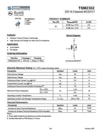
TSM2302 20V N-Channel MOSFET SOT-23 Pin Definition PRODUCT SUMMARY 1. Gate VDS (V) RDS(on)(m ) ID (A) 2. Source 3. Drain 65 @ VGS = 4.5V 2.8 20 95 @ VGS = 2.5V 2.0 Features Block Diagram Advance Trench Process Technology High Density Cell Design for Ultra Low On-resistance Application Load Switch PA Switch Ordering Information Part No.... See More ⇒
cj2302.pdf
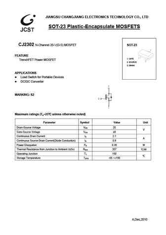
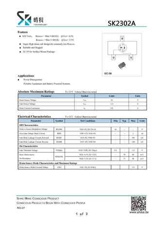
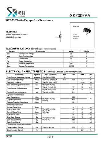
JIANGSU CHANGJIANG ELECTRONICS TECHNOLOGY CO., LTD SOT-23 Plastic-Encapsulate MOSFETS CJ2302 N-Channel 20-V(D-S) MOSFET SOT-23 FEATURE 1. GATE TrenchFET Power MOSFET 2. SOURCE 3. DRAIN APPLICATIONS Load Switch for Portable Devices DC/DC Converter MARKING S2 Maximum ratings (Ta=25 unless otherwise noted) Parameter Symbol Value Unit Drain-Source Voltage VDS ... See More ⇒
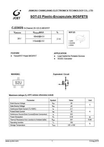
si2302.pdf
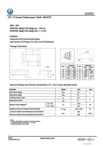
SI2302 20V N-Channel Enhancement Mode MOSFET VDS= 20V RDS(ON), Vgs@ 4.5V, Ids@ 3.6A 85m RDS(ON), Vgs@ 2.5V, Ids@ 2.0A 115m Features Advanced trench process technology High Density Cell Design For Ultra Low On-Resistance Package Dimensions D G S Millimeter Millimeter REF. REF. SOT-23 Min. Max. Min. Max. A 2.70 3.10 G 1.90 REF. B 2.40 2.80 H 1.00 1.30 C 1.4... See More ⇒
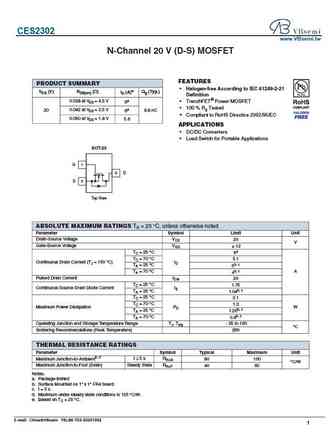
ces2302.pdf
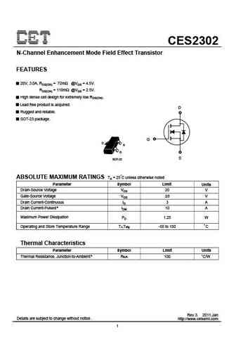
CES2302 N-Channel Enhancement Mode Field Effect Transistor FEATURES 20V, 3.0A, RDS(ON) = 72m @VGS = 4.5V. RDS(ON) = 110m @VGS = 2.5V. High dense cell design for extremely low RDS(ON). Lead free product is acquired. D Rugged and reliable. SOT-23 package. G D S G S SOT-23 ABSOLUTE MAXIMUM RATINGS TA = 25 C unless otherwise noted Parameter Symbol Limit Units Drain-Source V... See More ⇒
gm2302.pdf
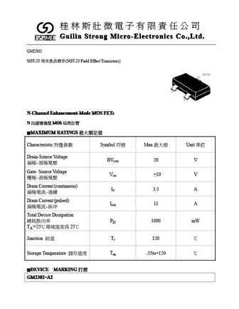
Guilin Strong Micro-Electronics Co.,Ltd. Guilin Strong Micro-Electronics Co.,Ltd. Guilin Strong Micro-Electronics Co.,Ltd. Guilin Strong Micro-Electronics Co.,Ltd. GM2302 SOT-23 (SOT-23 Field Effect Transistors) N-Channel Enhancement-Mode MOS FETs N-Channel Enhancement-Mode MOS FETs N-Channel Enhancement-Mode MOS FET... See More ⇒

g2302.pdf
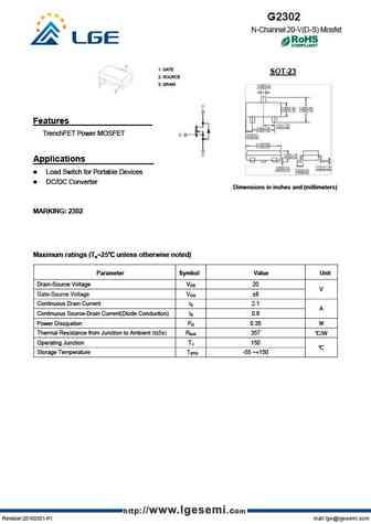
G2302 N-Channel 20-V(D-S) Mosfet 1. GATE SOT-23 2. SOURCE 3. DRAIN Features TrenchFET Power MOSFET Applications Load Switch for Portable Devices DC/DC Converter Dimensions in inches and (millimeters) MARKING 2302 Maximum ratings (Ta=25 unless otherwise noted) Parameter Symbol Value Unit Drain-Source Voltage VDS 20 V Gate-Source Voltage VGS 8 Continuous Dra... See More ⇒
wtc2302.pdf
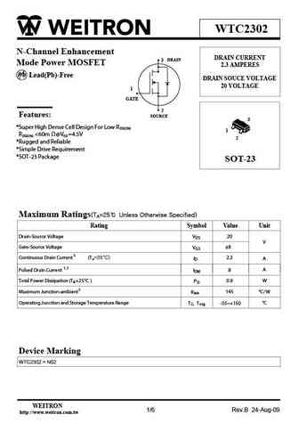
WTC2302 N-Channel Enhancement DRAIN CURRENT 3 DRAIN Mode Power MOSFET 2.3 AMPERES P b Lead(Pb)-Free DRAIN SOUCE VOLTAGE 20 VOLTAGE 1 GATE 2 Features SOURCE 3 *Super High Dense Cell Design For Low R DS(ON) 1 RDS(ON) ... See More ⇒
se2302.pdf
FM120-M WILLAS SE2302THRU SOT-23 Plastic-Encapsulate MOSFETS FM1200-M 1.0A SURFACE MOUNT SCHOTTKY BARRIER RECTIFIERS -20V- 200V SOD-123 PACKAGE Pb Free Product Package outline Features Batch process design, excellent power dissipation offers better reverse leakage current and thermal resistance. SOD-123H Low profile surface mounted application in order to optimiz... See More ⇒
aons32302.pdf
AONS32302 30V N-Channel MOSFET General Description Product Summary VDS 30V Trench Power MOSFET technology Low RDS(ON) ID (at VGS=10V) 220A Low Gate Charge RDS(ON) (at VGS=10V) ... See More ⇒
ap2302gn-hf.pdf
AP2302GN-HF Halogen-Free Product Advanced Power N-CHANNEL ENHANCEMENT MODE Electronics Corp. POWER MOSFET Capable of 2.5V gate drive BVDSS 20V Small package outline D RDS(ON) 85m Surface mount package ID 3.2A RoHS Compliant S SOT-23 G Description Advanced Power MOSFETs from APEC provide the designer with the best combination of fast switching, D low on-resistanc... See More ⇒
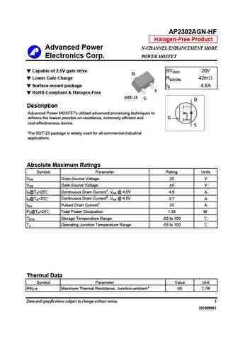
ap2302n-hf.pdf
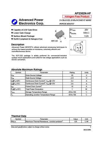
AP2302N-HF Halogen-Free Product Advanced Power N-CHANNEL ENHANCEMENT MODE Electronics Corp. POWER MOSFET Capable of 2.5V Gate Drive BVDSS 20V D Lower Gate Charge RDS(ON) 64m Surface Mount Package ID 3.2A S RoHS Compliant & Halogen-Free SOT-23S G D Description Advanced Power MOSFETs utilized advanced processing techniques to achieve the lowest possible on-resista... See More ⇒
ap2302agn.pdf
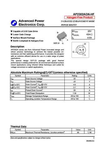
AP2302AGN-HF Halogen-Free Product Advanced Power N-CHANNEL ENHANCEMENT MODE Electronics Corp. POWER MOSFET Capable of 2.5V Gate Drive BVDSS 20V D Lower Gate Charge RDS(ON) 42m Surface Mount Package ID 4.6A S RoHS Compliant & Halogen-Free SOT-23 G D Description AP2302A series are from Advanced Power innovated design and silicon process technology to achieve the l... See More ⇒
ap2302gn.pdf
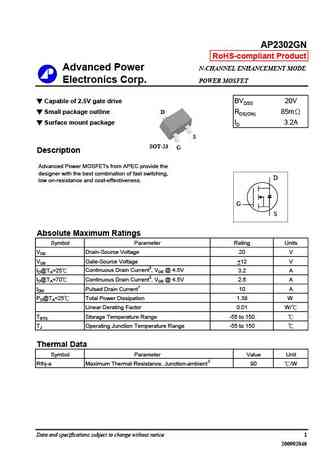
AP2302GN RoHS-compliant Product Advanced Power N-CHANNEL ENHANCEMENT MODE Electronics Corp. POWER MOSFET Capable of 2.5V gate drive BVDSS 20V Small package outline D RDS(ON) 85m Surface mount package ID 3.2A S SOT-23 G Description Advanced Power MOSFETs from APEC provide the designer with the best combination of fast switching, D low on-resistance and cost-effectiven... See More ⇒
ap2302agn-hf.pdf
AP2302AGN-HF Halogen-Free Product Advanced Power N-CHANNEL ENHANCEMENT MODE Electronics Corp. POWER MOSFET Capable of 2.5V gate drive BVDSS 20V D Lower Gate Charge RDS(ON) 42m Surface mount package ID 4.6A S RoHS Compliant & Halogen-Free SOT-23 G D Description Advanced Power MOSFETs utilized advanced processing techniques to achieve the lowest possible on-resist... See More ⇒
am2302ne.pdf
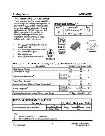
Analog Power AM2302NE N-Channel 20-V (D-S) MOSFET These miniature surface mount MOSFETs utilize a high cell density trench process to PRODUCT SUMMARY provide low rDS(on) and to ensure minimal VDS (V) rDS(on) ( ) ID (A) power loss and heat dissipation. Typical applications are DC-DC converters and 0.076 @ VGS = 4.5V 3.4 20 power management in portable and 0.103 @ VGS = 2.5V 2... See More ⇒
am2302n.pdf
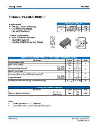
Analog Power AM2302N N-Channel 20-V (D-S) MOSFET PRODUCT SUMMARY Key Features rDS(on) (m ) VDS (V) ID(A) Low r trench technology DS(on) 76 @ VGS = 4.5V 3.4 Low thermal impedance 20 103 @ VGS = 2.5V 3.0 Fast switching speed Typical Applications White LED boost converters Automotive Systems Industrial DC/DC Conversion Circuits ABSOLUTE MAXIMUM... See More ⇒
afn2302as.pdf
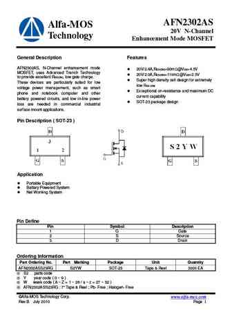
AFN2302AS Alfa-MOS 20V N-Channel Technology Enhancement Mode MOSFET General Description Features AFN2302AS, N-Channel enhancement mode 20V/2.4A,RDS(ON)=90m @VGS=4.5V MOSFET, uses Advanced Trench Technology 20V/2.0A,RDS(ON)=110m @VGS=2.5V to provide excellent RDS(ON), low gate charge. Super high density cell design for extremely These devices are particularly suite... See More ⇒
afn2302s.pdf
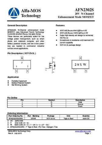
AFN2302S Alfa-MOS 20V N-Channel Technology Enhancement Mode MOSFET General Description Features AFN2302S, N-Channel enhancement mode 20V/3.6A,RDS(ON)=85m @VGS=4.5V MOSFET, uses Advanced Trench Technology 20V/3.2A,RDS(ON)=100m @VGS=2.5V to provide excellent RDS(ON), low gate charge. Super high density cell design for extremely These devices are particularly suited ... See More ⇒
si2302a.pdf
Shenzhen Tuofeng Semiconductor Technology Co., Ltd SI2302A N-Channel 1.25-W, 2.5-V MOSFET PRODUCT SUMMARY VDS (V) rDS(on) (W) ID (A) 0.040 @ VGS = 4.5 V 3.0 20 20 0.060 @ V 2.0 GS = 2.5 V (SOT-23) G 1 3 D S 2 Top View (A2)* SI2302A ABSOLUTE MAXIMUM RATINGS (TA = 25_C UNLESS OTHERWISE NOTED) Parameter Symbol Limit Unit Drain-Source Voltage VDS 20 V V Gate-Source Voltage VG... See More ⇒
si2302 a2shb.pdf
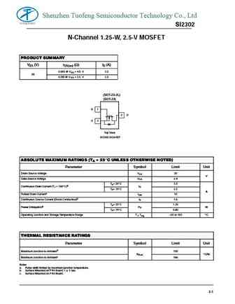
Shenzhen Tuofeng Semiconductor Technology Co., Ltd SI2302 N-Channel 1.25-W, 2.5-V MOSFET PRODUCT SUMMARY VDS (V) rDS(on) (W) ID (A) 0.065 @ VGS = 4.5 V 3.0 20 20 0.090 @ V 2.0 GS = 2.5 V (SOT-23-3L) (SOT-23) G 1 3 D S 2 Top View SI2302 (A2sHB)* ABSOLUTE MAXIMUM RATINGS (TA = 25_C UNLESS OTHERWISE NOTED) Parameter Symbol Limit Unit Drain-Source Voltage VDS 20 V V Gate-Sou... See More ⇒
mtn2302n3.pdf
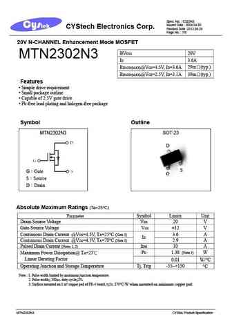
Spec. No. C323N3 Issued Date 2004.04.05 CYStech Electronics Corp. Revised Date 2012.06.26 Page No. 1/8 20V N-CHANNEL Enhancement Mode MOSFET BVDSS 20V MTN2302N3 ID 3.6A 29m (typ.) RDSON(MAX)@VGS=4.5V, ID=3.6A 39m (typ.) RDSON(MAX)@VGS=2.5V, ID=3.1A Features Simple drive requirement Small package outline Capable of 2.5V gate drive Pb-free le... See More ⇒
mtn2302v3.pdf
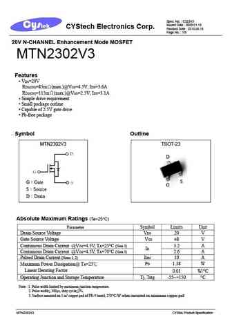
Spec. No. C323V3 Issued Date 2009.01.19 CYStech Electronics Corp. Revised Date 2010.06.18 Page No. 1/9 20V N-CHANNEL Enhancement Mode MOSFET MTN2302V3 Features V =20V DS R =85m (max.)@V =4.5V, I =3.6A DS(ON) GS DS R =115m (max.)@V =2.5V, I =3.1A DS(ON) GS DS Simple drive requirement Small package outline Capable of 2.5V gate drive ... See More ⇒
sts2302a.pdf
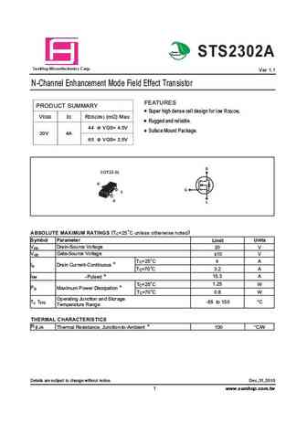
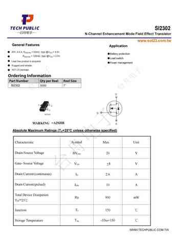
Green Product STS2302A a S mHop Microelectronics C orp. Ver 1.1 N-Channel Enhancement Mode Field Effect Transistor FEATURES PRODUCT SUMMARY Super high dense cell design for low RDS(ON). VDSS ID RDS(ON) (m ) Max Rugged and reliable. 44 @ VGS= 4.5V Suface Mount Package. 20V 4A 65 @ VGS= 2.5V D S OT23-3L D G S G S (TC=25 C unless otherwise noted) ABSOLUTE MAXIMUM RATINGS ... See More ⇒
ssf2302.pdf
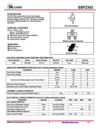
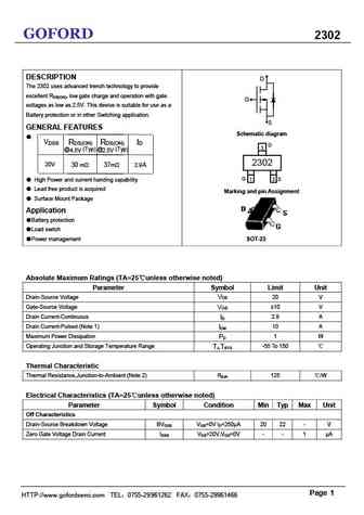
SSF2302 D DESCRIPTION The SSF2302 uses advanced trench technology to provide excellent RDS(ON), low gate charge and operation G with gate voltages as low as 2.5V. This device is suitable for use as a Battery protection or in other Switching application. S Schematic diagram GENERAL FEATURES VDS = 20V,ID = 2.4A D 3 RDS(ON) ... See More ⇒
cs2302 sot-23.pdf
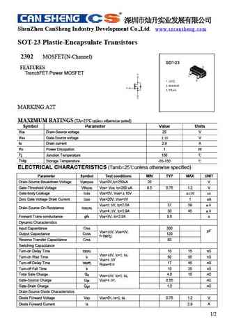
ShenZhen CanSheng Industry Development Co.,Ltd. www.szcansheng.com SOT-23 Plastic-Encapsulate Transistors 2302 MOSFET(N-Channel) FEATURES TrenchFET Power MOSFET MARKING A2T MAXIMUM RATINGS (TA=25 unless otherwise noted) Symbol Parameter Value Units VDS Drain-Source voltage 20 V VGS Gate-Source voltage 10 V ID Drain current 2.9... See More ⇒
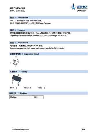
brcs2302ama.pdf
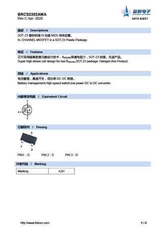
BRCS2302AMA Rev.C Apr.-2020 DATA SHEET / Descriptions SOT-23 N MOS N- CHANNEL MOSFET in a SOT-23 Plastic Package. / Features R SOT-23 DS(ON) Super high dense cell design for low RDS(ON),SOT-23 package. Halogen-free Product. / Applicati... See More ⇒
si2302.pdf
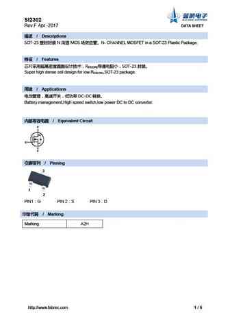
SI2302 Rev.F Apr.-2017 DATA SHEET / Descriptions SOT-23 N MOS N- CHANNEL MOSFET in a SOT-23 Plastic Package. / Features R SOT-23 DS(ON) Super high dense cell design for low RDS(ON),SOT-23 package. / Applications ... See More ⇒
mmftn2302.pdf
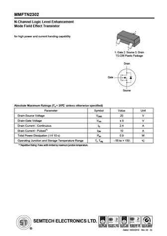
MMFTN2302 N-Channel Logic Level Enhancement Mode Field Effect Transistor for high power and current handing capability 1. Gate 2. Source 3. Drain TO-236 Plastic Package Drain Gate Source Absolute Maximum Ratings (Ta = 25 unless otherwise specified) Parameter Symbol Value Unit Drain-Source Voltage VDSS 20 V Drain-Gate Voltage VGS 8 V Drain Current - Continuous ID 2.4 A ... See More ⇒
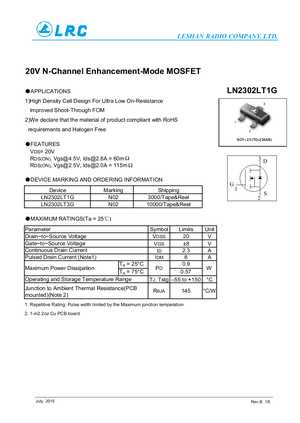
ln2302blt1g s-ln2302blt1g.pdf
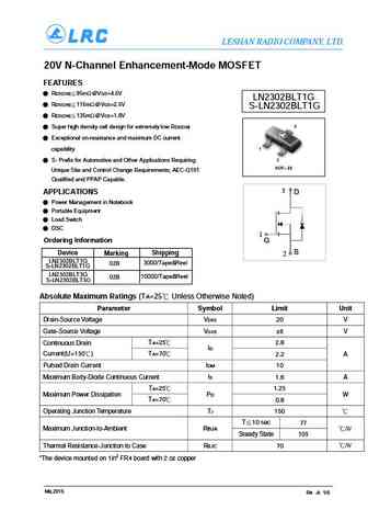
LESHAN RADIO COMPANY, LTD. 20V N-Channel Enhancement-Mode MOSFET FEATURES RDS(ON) 85m @VGS=4.5V LN2302BLT1G RDS(ON) 115m @VGS=2.5V S-LN2302BLT1G RDS(ON) 135m @VGS=1.8V 3 Super high density cell design for extremely low RDS(ON) Exceptional on-resistance and maximum DC current capability 1 2 S- Prefix for Automotive and Other Applications Re... See More ⇒
sm2302nsa.pdf
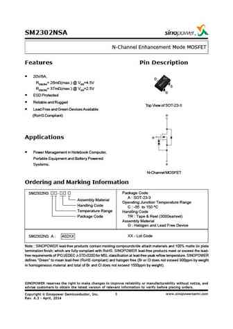
SM2302NSA N-Channel Enhancement Mode MOSFET Features Pin Description 20V/6A, D RDS(ON)= 26m (max.) @ VGS=4.5V S RDS(ON)= 37m (max.) @ VGS=2.5V G ESD Protected Reliable and Rugged Top View of SOT-23-3 Lead Free and Green Devices Available D (RoHS Compliant) G Applications Power Management in Notebook Computer, Portable Equipment and Battery Powered S Systems. N-Chan... See More ⇒
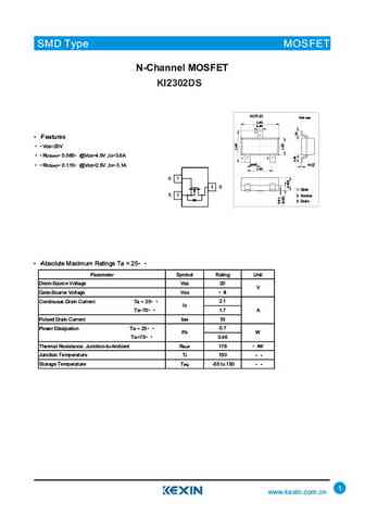
ki2302ds.pdf
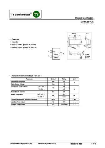
SMD Type SMD Type IC Product specification KI2302DS SOT-23 Unit mm +0.1 2.9-0.1 +0.1 0.4-0.1 3 Features VDS=20V RDS(on)= 0.085 @VGS=4.5V ,ID=3.6A 1 2 +0.1 +0.05 0.95-0.1 0.1-0.01 RDS(on)= 0.115 @VGS=2.5V ,ID= 3.1A +0.1 1.9-0.1 G 1 3 D 1.Base 1. Gate S 2 2.Emitter 2. Source 3. Drain 3.collector Absolute Maximum Ratings Ta = 25 Parameter ... See More ⇒
dmg2302u.pdf
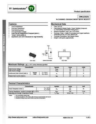
Product specification DMG2302U N-CHANNEL ENHANCEMENT MODE MOSFET Features Mechanical Data Low On-Resistance Case SOT-23 Low Input Capacitance Case Material Molded Plastic, Green Molding Compound. UL Flammability Classification Rating 94V-0 Fast Switching Speed Moisture Sensitivity Level 1 per J-STD-020D Low Input/Output Leakage Terminal... See More ⇒
ftk2302.pdf
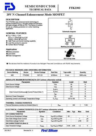
SEMICONDUCTOR FTK2302 TECHNICAL DATA 20V N-Channel Enhancement-Mode MOSFET D DESCRIPTION The FTK2302 uses advanced trench technology to provide excellent RDS(ON), low gate charge and operation G with gate voltages as low as 2.5V. This device is suitable for use as a Battery protection or in other Switching application. S Schematic diagram GENERAL FEATURES VDS = 20V,I... See More ⇒
si2302 ki2302.pdf
SMD Type MOSFET N-Channel Enhancement MOSFET SI2302 (KI2302) SOT-23-3 Unit mm +0.2 2.9 -0.1 +0.1 0.4-0.1 3 Features VDS=20V RDS(on)= 85m @VGS=4.5V ,ID=3.6A RDS(on)= 115m @VGS=2.5V ,ID=3.1A 1 2 +0.02 +0.1 0.15 -0.02 0.95 -0.1 +0.1 1.9 -0.2 G 1 3 D 1. Gate S 2 2. Source 3. Drain Absolute Maximum Ratings Ta = 25 Parameter Symbol Rating Unit Dr... See More ⇒
si2302ds-3.pdf
SMD Type MOSFET N-Channel Enhancement MOSFET SI2302DS (KI2302DS) SOT-23-3 Unit mm +0.2 2.9 -0.1 +0.1 0.4-0.1 3 Features VDS=20V RDS(on)= 85m @VGS=4.5V ,ID=3.6A RDS(on)= 115m @VGS=2.5V ,ID=3.1A 1 2 +0.02 +0.1 0.15 -0.02 0.95 -0.1 +0.1 1.9 -0.2 G 1 3 D 1. Gate S 2 2. Source 3. Drain Absolute Maximum Ratings Ta = 25 Parameter Symbol Rating Un... See More ⇒
si2302ds.pdf
SMD Type MOSFET N-Channel Enhancement MOSFET SI2302DS (KI2302DS) SOT-23 Unit mm +0.1 2.9 -0.1 0.4+0.1 -0.1 Features 3 VDS=20V RDS(on)= 85m @VGS=4.5V ,ID=3.6A RDS(on)= 115m @VGS=2.5V ,ID=3.1A 1 2 +0.1 +0.05 0.95 -0.1 0.1-0.01 +0.1 1.9 -0.1 G 1 1.Gate 3 D 2.Source S 2 3.Drain Absolute Maximum Ratings Ta = 25 Parameter Symbol Rating Unit Dr... See More ⇒
ki2302ds.pdf
SMD Type Diodes SMD Type MOSFET SMD Type MOSFET N-Channel MOSFET KI2302DS SOT-23 Unit mm +0.1 2.9-0.1 +0.1 0.4-0.1 3 Features VDS=20V RDS(on)= 0.085 @VGS=4.5V ,ID=3.6A 1 2 +0.1 +0.05 0.95-0.1 0.1-0.01 RDS(on)= 0.115 @VGS=2.5V ,ID= 3.1A +0.1 1.9-0.1 G 1 3 D 1.Base 1. Gate S 2 2.Emitter 2. Source 3. Drain 3.collector Absolute Maximum Ratings... See More ⇒
blm2302.pdf
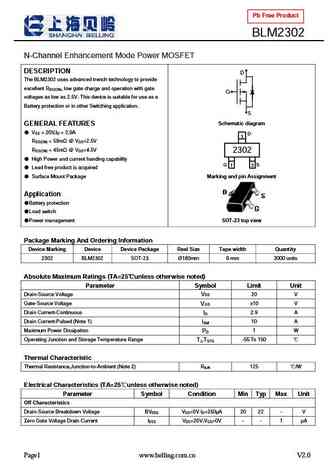
Pb Free Product BLM2302 N-Channel Enhancement Mode Power MOSFET DESCRIPTION D The BLM2302 uses advanced trench technology to provide excellent R , low gate charge and operation with gate DS(ON) G voltages as low as 2.5V. This device is suitable for use as a Battery protection or in other Switching application. S Schematic diagram GENERAL FEATURES V = 20V,I = 2.9A D... See More ⇒
cht2302wgp.pdf
CHENMKO ENTERPRISE CO.,LTD CHT2302WGP SURFACE MOUNT N-Channel Enhancement Mode Field Effect Transistor VOLTAGE 20 Volts CURRENT 2.8 Ampere APPLICATION * Servo motor control. * Power MOSFET gate drivers. * Other switching applications. SC-70/SOT-323 FEATURE * Small surface mounting type. (SC-70/SOT-323) * High density cell design for low RDS(ON). * Suitable for high packing dens... See More ⇒
cht2302gp.pdf
CHENMKO ENTERPRISE CO.,LTD CHT2302GP SURFACE MOUNT N-Channel Enhancement Mode Field Effect Transistor VOLTAGE 20 Volts CURRENT 2.8 Ampere APPLICATION * Servo motor control. * Power MOSFET gate drivers. * Other switching applications. SOT-23 FEATURE * Small surface mounting type. (SOT-23) * High density cell design for low RDS(ON). * Suitable for high packing density. * Rugged ... See More ⇒
ctn2302.pdf
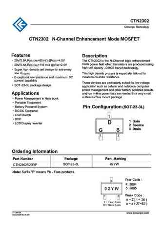
CTN2302 Crownpo Technology CTN2302 N-Channel Enhancement Mode MOSFET Features Description 20V/2.8A,RDS(ON)=85m @VGS=4.5V The CTN2302 is the N-Channel logic enhancement 20V/2.4A,R =115 m @VGS=2.5V mode power field effect transistors are produced using DS(ON) high cell density , DMOS trench technology. Super high density cell design for extremely low RDS(ON) Exc... See More ⇒
bl2302.pdf
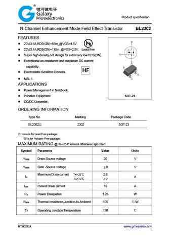
Product specification N-Channel Enhancement Mode Field Effect Transistor BL2302 FEATURES 20V/3.6A,RDS(ON)=85m_@VGS=4.5V. Pb 20V/3.1A,RDS(ON)=115m_@VGS=2.5V. Lead-free Super high density cell design for extremely low RDS(ON). Exceptional on-resistance and maximum DC current capability. Electrostatic Sensitive Devices. MSL 1. APPLICATIONS Powe... See More ⇒
gsm2302as.pdf
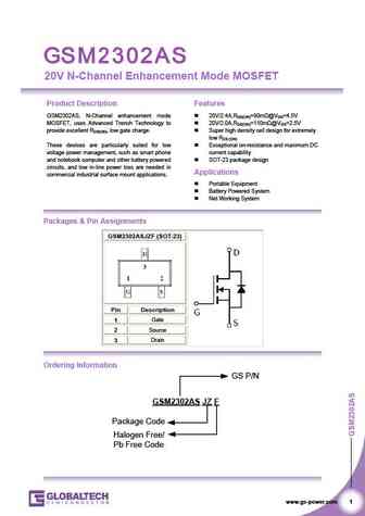
20V N-Channel Enhancement Mode MOSFET Product Description Features GSM2302AS, N-Channel enhancement mode 20V/2.4A,RDS(ON)=90m @VGS=4.5V MOSFET, uses Advanced Trench Technology to 20V/2.0A,RDS(ON)=110m @VGS=2.5V provide excellent RDS(ON), low gate charge. Super high density cell design for extremely low RDS (ON) These devices are particularly suited for low Exceptional on-... See More ⇒
gsm2302s.pdf
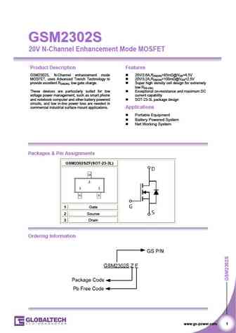
GSM2302S GSM2302S 20V N-Channel Enhancement Mode MOSFET Product Description Features GSM2302S, N-Channel enhancement mode 20V/3.6A,RDS(ON)=85m @VGS=4.5V MOSFET, uses Advanced Trench Technology to 20V/3.2A,RDS(ON)=100m @VGS=2.5V provide excellent RDS(ON), low gate charge. Super high density cell design for extremely low RDS (ON) These devices are particularly suited for ... See More ⇒
kia2302.pdf
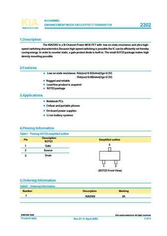
N-CHANNEL ENHANCEMENT MODE FIELD EFFECT TRANSISTOR KIA 2302 SEMICONDUCTORS 1.Description The KIA2302 is a N-Channel Power MOS FET with low on-state resistance and ultra high- speed switching characteristics.Because high-speed switching is possible,the IC can be efficiently set thereby saving energy. In order to counter static, a gate protect diode is built-in. The small SOT23 package ma... See More ⇒
me2302.pdf
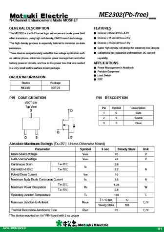
ME2302(Pb-free) N-Channel Enhancement Mode MOSFET GENERAL DESCRIPTION FEATURES The ME2302 is the N-Channel logic enhancement mode power field RDS(ON) 85m @VGS=4.5V effect transistors, using high cell density, DMOS trench technology. RDS(ON) 115m @VGS=2.5V This high density process is especially tailored to minimize on-state RDS(ON) 135m @VGS=1.8V resistance. ... See More ⇒
me2302 me2302-g.pdf
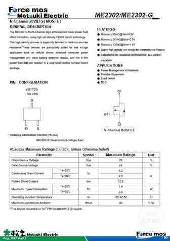
ME2302/ME2302-G N-Channel 20V(D-S) MOSFET GENERAL DESCRIPTION FEATURES The ME2302 is the N-Channel logic enhancement mode power field RDS(ON) 85m @VGS=4.5V effect transistors, using high cell density, DMOS trench technology. RDS(ON) 115m @VGS=2.5V This high density process is especially tailored to minimize on-state RDS(ON) 130m @VGS=1.8V resistance.T... See More ⇒
mmn2302.pdf
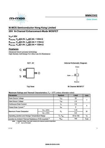
MMN2302 Data Sheet M-MOS Semiconductor Hong Kong Limited 20V N-Channel Enhancement-Mode MOSFET VDS= 20V RDS(ON), Vgs@4.5V, Ids@2.8A = 60m RDS(ON), Vgs@2.5V, Ids@2.0A = 115m RDS(ON), Vgs@1.8V, Ids@2.0A = 130m Features Advanced trench process technology High Density Cell Design For Ultra Low On-Resistance SOT -23 Internal Schematic Diagram Drain Gate Source Top View N-C... See More ⇒
nce2302.pdf
Pb Free Product http //www.ncepower.com NCE2302 NCE N-Channel Enhancement Mode Power MOSFET Description D The NCE2302 uses advanced trench technology to provide excellent RDS(ON), low gate charge and operation with gate G voltages as low as 2.5V. This device is suitable for use as a Battery protection or in other Switching application. S Schematic diagram General Features ... See More ⇒
nce2302c.pdf
Pb Free Product http //www.ncepower.com NCE2302C NCE N-Channel Enhancement Mode Power MOSFET Description The NCE2302C uses advanced trench technology to provide excellent RDS(ON), low gate charge and operation with gate voltages as low as 2.5V. This device is suitable for use as a Battery protection or in other Switching application. General Features Schematic diagram VD... See More ⇒
nce2302b.pdf
Pb Free Product http //www.ncepower.com NCE2302B NCE N-Channel Enhancement Mode Power MOSFET Description The NCE2302B uses advanced trench technology to provide excellent RDS(ON), low gate charge and operation with gate voltages as low as 2.5V. This device is suitable for use as a Battery protection or in other Switching application. Schematic diagram General Features VD... See More ⇒
stn2302.pdf
STN2302 20V N-Channel Enhancement Mode MOSFET DESCRIPTION FEATURE The STN2302 is the N-Channel logic enhancement 20V/4.0A, RDS(ON) =50m (typ.)@VGS =4.5V mode power field effect transistor is produced using 20V/3.0A, RDS(ON) =65m (typ.)@VGS =2.5V high cell density. advanced trench technology to provide excellent RDS(ON). low gate charge and Super high densi... See More ⇒
shd230209.pdf
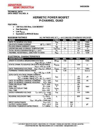
SENSITRON SHD230209 SEMICONDUCTOR TECHNICAL DATA DATA SHEET 318, REV. A HERMETIC POWER MOSFET P-CHANNEL QUAD FEATURES -100 Volt, 0.60 Ohm, -3.5A MOSFET Fast Switching Low RDS (on) Equivalent to IRF9120 Series MAXIMUM RATINGS ALL RATINGS ARE AT TC = 25 C UNLESS OTHERWISE SPECIFIED. RATING SYMBOL MIN. TYP. MAX. UNITS GATE TO SOURCE VOLTAGE VGS - - 20 Volts ID - ... See More ⇒
shd230202.pdf
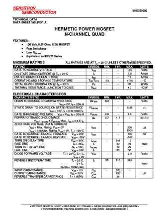
SENSITRON SHD230202 SEMICONDUCTOR TECHNICAL DATA DATA SHEET 319, REV. A HERMETIC POWER MOSFET N-CHANNEL QUAD FEATURES 100 Volt, 0.35 Ohm, 6.2A MOSFET Fast Switching Low RDS (on) Equivalent to IRF120 Series MAXIMUM RATINGS ALL RATINGS ARE AT TC = 25 C UNLESS OTHERWISE SPECIFIED. RATING SYMBOL MIN. TYP. MAX. UNITS GATE TO SOURCE VOLTAGE VGS - - 20 Volts ID - - 6... See More ⇒
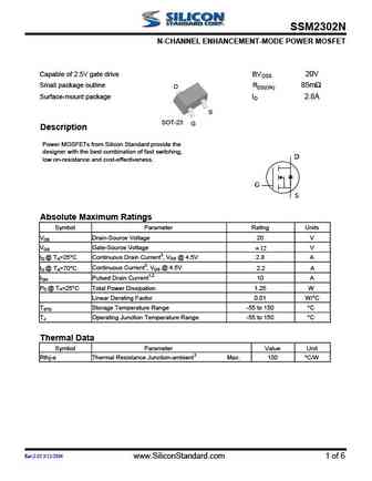
ssm2302gn.pdf
SSM2302N N-CHANNEL ENHANCEMENT-MODE POWER MOSFET Capable of 2.5V gate drive BVDSS 20V Small package outline RDS(ON) 85m D Surface-mount package ID 2.8A S SOT-23 G Description Power MOSFETs from Silicon Standard provide the designer with the best combination of fast switching, D low on-resistance and cost-effectiveness. G S Absolute Maximum Ratings Symbol Parameter Rating Uni... See More ⇒
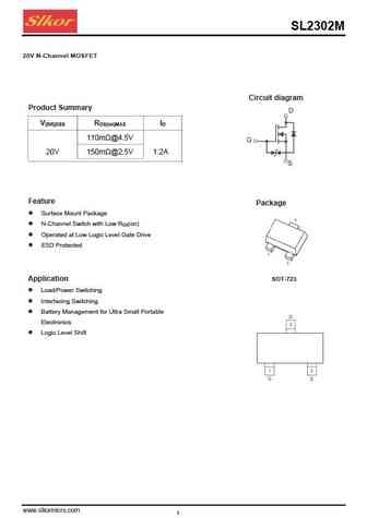
sl2302m.pdf
SL2302M 20V N-Channel MOSFET Circuit diagram Product Summary V R I (BR)DSS DS(on)MAX D 110m @4.5V 20V 150m @2.5V 1.2A Feature Package Surface Mount Package N-Channel Switch with Low R (on) DS Operated at Low Logic Level Gate Drive ESD Protected Application SOT-723 Load/Power Switching Interfacing Switching Battery Management for Ultra Small Portab... See More ⇒
sl2302s.pdf
SL2302S SOT-23 Package Information Dimensions in Millimeters Symbol MIN. MAX. A 0.900 1.150 A1 0.000 0.100 A2 0.900 1.050 b 0.300 0.500 c 0.080 0.150 D 2.800 3.000 E 1.200 1.400 E1 2.250 2.550 e 0.950TYP e1 1.800 2.000 L 0.550REF L1 0.300 0.500 0 8 www.slkormicro.com 3 ... See More ⇒
sl2302.pdf
SL2302 N-Channel Power MOSFET General Features VDS = 20V,ID = 2.8 A RDS(ON) ... See More ⇒
st2302.pdf
ST2302 N Channel Enhancement Mode MOSFET 3.6A DESCRIPTION ST2302 is the N-Channel logic enhancement mode power field effect transistor which is produced using high cell density, DMOS trench technology.This high density process is especially tailored to minimize on-state resistance.These devices are particularly suited for low voltage application such as cellular phone and noteboo... See More ⇒
tp2302nr.pdf
TP2302NR N-CHANNEL ENHANCEMENT MODE FIELD EFFECT TRANSISTOR FEATURES HIGH DENSITY CELL DESIGN FOR ULTRA LOW ON-RESISTANCE IMPROVED SHOOT-THROUGH FOM BOTH NORMAL AND PB FREE PRODUCT ARE AVAILABLE NORMAL 80 95% SN, 5 20% PB PB FREE 99% SN ABOVE MECHANICAL DATA WE DECLARE THAT THE MATERIAL OF PRODUCT COMPLIANCE WITH ROHS REUIREMENTS. Pb Free TP2302NR... See More ⇒
si2302a.pdf
R UMW UMW SI2302A UMW SI2302A UMW SI2302A N-Channel Enhancement MOSFET Features SOT 23 VDS=20V RDS(on)= 85m @VGS=4.5V ,ID=3.6A RDS(on)= 115m @VGS=2.5V ,ID=3.1A Marking 1. GATE 2. SOURCE G 1 3. DRAIN 3 D S 2 Absolute Maximum Ratings Ta = 25 Parameter Symbol Rating Unit Drain-Source Voltage VDS 20 V Gate-Source Voltage VGS 8 Ta=25 2.... See More ⇒
si2302b.pdf
R UMW UMW SI2302B UMW SI2302B UMW SI2302B SOT-23 Plastic-Encapsulate MOSFETS N-Channel 20-V(D-S) MOSFET UMW SI2302B SOT 23 ID V(BR)DSS RDS(on)MAX 80 m @4.5V 20V 2.5A 100m @2.5V 1. GATE 2. SOURCE 3. DRAIN FEA TURE APPLICATION Load Switch for Portable Devices TrenchFET Power MOSFET DC/DC Converter MARKING Equivalent Circuit A2SHB Maximum rating... See More ⇒
atm2302bnsa.pdf
ATM2302BNSA N-Channel Enhancement Mode Field Effect Transistor Drain-Source Voltage 20V Drain Current 3A Features Trench Power LV MOSFET technology High power and current handing capability R ... See More ⇒
atm2302nsa.pdf
ATM2302NSA N-Channel Enhancement Mode Field Effect Transistor Drain-Source Voltage 20V Drain Current 3.3A Features Trench FET Power MOSFET Excellent R and Low Gate Charge DS(on) R ... See More ⇒

as2302.pdf
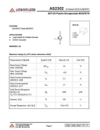
AS2302 N-Channel 20V(D-S) MOSFET SOT-23 Plastic-Encapsulate MOSFETS SOT-23 FEATURE TrenchFET Power MOSFET 1. GATE APPLICATIONS 2. SOURCE 3. DRAIN Load Switch for Portable Devices DC/DC Converter MARKING A2 Maximum ratings (Ta=25 unless otherwise noted) Characteristic Symbol Max Unit Drain-Source Voltage BVDSS 20 V - ... See More ⇒
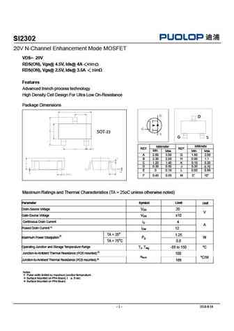
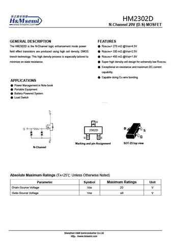
si2302s.pdf
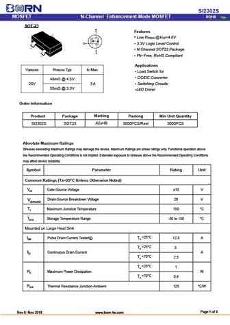
SI2302S MOSFET ROHS N-Channel Enhancement-Mode MOSFET SOT-23 - Features Low RDS(on) @VGS=4.5V 3.3V Logic Level Control N Channel SOT23 Package Pb-Free, RoHS Compliant Applications V R Typ I Max (BR)DSS DS(ON) D Load Switch for DC/DC Converter 48m @ 4.5V Switching Circuits 20V 3 A 55m @ 3.3V LED Driver Order Information Mar... See More ⇒
si2302.pdf
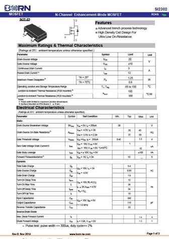
SI2302 MOSFET ROHS N-Channel Enhancement-Mode MOSFET SOT-23 - Features Advanced trench process technology High Density Cell Design For Ultra Low On-Resistance Maximum Ratings & Thermal Characteristics (Ratings at 25 ambient temperature unless otherwise specified.) Parameter Symbol Limit Unit Drain-Source Voltage VDS 20 V Gate-Source Voltage VGS 10 Continuous... See More ⇒
ctz2302a.pdf
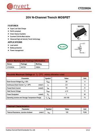
nvert CTZ2302A Suzhou Convert Semiconductor Co ., Ltd. 20V N-Channel Trench MOSFET FEATURES Super Low Gate Charge RoHS compliant Green Device Available Excellent CdV/dt effect decline Advanced high cell density Trench technology APPLICATIONS Load switch Battery protection Power management Device Marking and Package Information Device Package Markin... See More ⇒
fs2302a.pdf
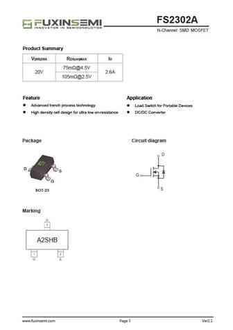
FS2302A N-Channel SMD MOSFET Product Summary V R I (BR)DSS DS(on)MAX D 75m @4.5V 20V 2.6A 105m @2.5V Feature Application Advanced trench process technology Load Switch for Portable Devices High density cell design for ultra low on-resistance DC/DC Converter Package Circuit diagram D S G SOT-23 Marking A2SHB www.fuxinsemi.com Page 1 Ver2.1 FS2302A N-Channel SMD MOSFE... See More ⇒
as2302.pdf
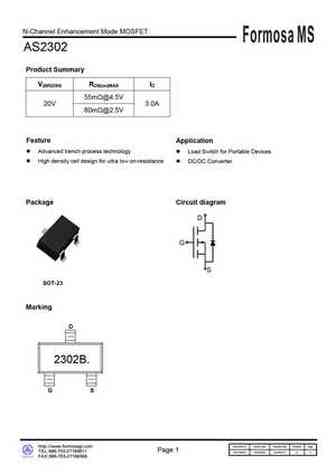
N-Channel Enhancement Mode MOSFET Formosa MS AS2302 Product Summary V(BR)DSS RDS(on)MAX ID 55m @4.5V 20V 3.0A 80m @2.5V Feature Application Advanced trench process technology Load Switch for Portable Devices High density cell design for ultra low on-resistance DC/DC Converter Package Circuit diagram SOT-23 Marking 2302B. Document ID http //www.formosagr.com Doc... See More ⇒


gp2302.pdf
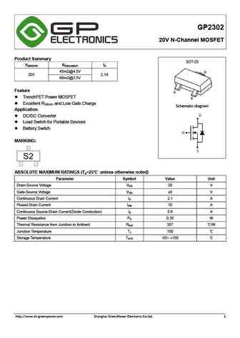
GP2302 20V N-Channel MOSFET Product Summary SOT-23 V R I (BR)DSS DS(on)MAX D 45m @4.5V 20V 2.1A 60m @2.5V Feature TrenchFET Power MOSFET Excellent RDS(on) and Low Gate Charge Schematic diagram Application DC/DC Converter Load Switch for Portable Devices Battery Switch MARKING ABSOLUTE MAXIMUM RATINGS (Ta=25 unless otherwise noted) P... See More ⇒
si2302.pdf
Plastic-Encapsulate Mosfets FEATURES SI2302 High dense cell design for extremely low RDS(ON) N-Channel MOSFET Rugged and reliable Case Material Molded Plastic. Absolute Maximum Ratings (TA=25oC, unless otherwise noted) Parameter Symbol Ratings Unit Drain-Source Voltage VDS 20 V Gate-source Voltage VGS 8 V 1.Gate 2.Source Drain Current (Continuous) ID 2.1 A SOT-23 3.Drain a Drai... See More ⇒
hss2302b.pdf

HSS2302B N-Ch 20V Fast Switching MOSFETs Product Summary Description The HSS2302B is the high cell density trenched VDS 20 V N-ch MOSFETs, which provides excellent RDSON and efficiency for most of the small RDS(ON),typ 46 m power switching and load switch applications. ID 3 A The HSS2302B meets the RoHS and Green Product requirement with full function reliability ap... See More ⇒
hss2302a.pdf
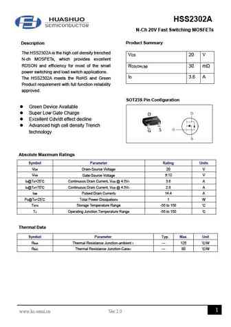
HSS2302A N-Ch 20V Fast Switching MOSFETs Product Summary Description The HSS2302A is the high cell density trenched VDS 20 V N-ch MOSFETs, which provides excellent RDSON and efficiency for most of the small RDS(ON),typ 30 m power switching and load switch applications. ID 3.6 A The HSS2302A meets the RoHS and Green Product requirement with full function reliability ... See More ⇒
hx2302a.pdf

SOT-23 Plastic-Encapsulate Transistors HX2302A MOSFET(N-Channel) FEATURES TrenchFET Power MOSFET MARKING A2SHB MAXIMUM RATINGS (TA=25 unless otherwise noted) Symbol Parameter Value Units VDS Drain-Source voltage 20 V VGS Gate-Source voltage 12 V ID Drain current 2.5 A PD Power Dissipation 0.9 W Tj Junction Temperature 150 Tstg Storage Temperature -55-150 ELECTRICAL C... See More ⇒
hx2302.pdf
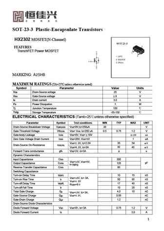
SOT-23-3 Plastic-Encapsulate Transistors HX2302 MOSFET(N-Channel) FEATURES TrenchFET Power MOSFET MARKING A2SHB MAXIMUM RATINGS (TA=25 unless otherwise noted) Symbol Parameter Value Units VDS Drain-Source voltage 20 V VGS Gate-Source voltage 8 V ID Drain current 3.0 A PD Power Dissipation 1 W Tj Junction Temperature 150 Tstg Storage Temperature -55-150 EL... See More ⇒
hd2302.pdf
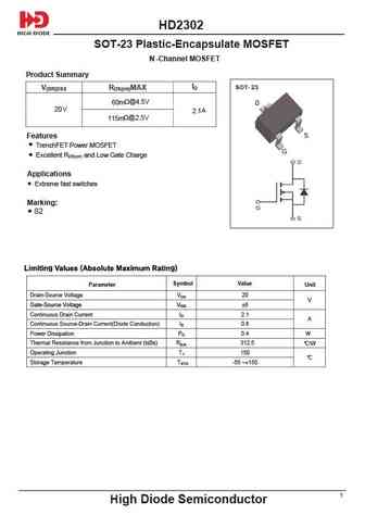
HD2302 SOT-23 Plastic-Encapsulate MOSFET N -Channel MOSFET roduct Summary P ID SOT- 23 V(BR)DSS RDS(on)MAX 60m @4.5V D 20V 2.1A 115m @2.5V S Features TrenchFET Power MOSFET G Excellent RDS(on) and Low Gate Charge Applications Extreme fast switches Marking S2 Symbol Value Parameter Unit Drain-Source Voltage VDS 20 V Gate-S... See More ⇒
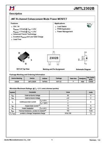
jmtl2302b.pdf
JMTL2302B Description JMT N-channel Enhancement Mode Power MOSFET Features Applications 20V, 3A Load Switch RDS(ON) ... See More ⇒
jmtl2302a.pdf
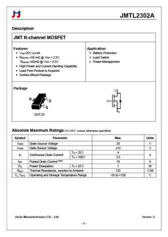
JMTL2302A Description JMT N-channel MOSFET Features Application V =20V, I =4A Battery Protection DS D R ... See More ⇒
jmtj2302c.pdf
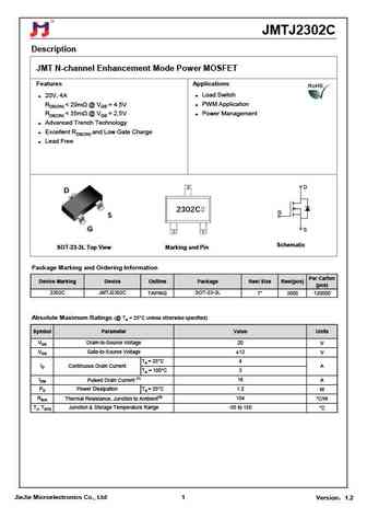
JMTJ2302C Description JMT N-channel Enhancement Mode Power MOSFET Features Applications 20V, 4A Load Switch RDS(ON) ... See More ⇒
jmtl2302c.pdf
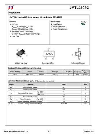
JMTL2302C Description JMT N-channel Enhancement Mode Power MOSFET Features Applications 20V, 4A Load Switch RDS(ON) ... See More ⇒
jst2302h.pdf
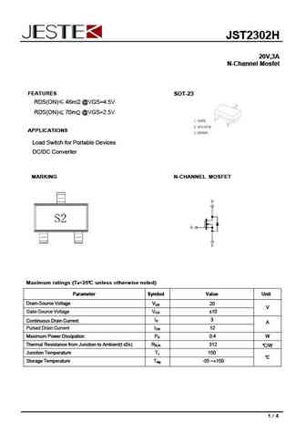
JST2302H 20V,3A N-Channel Mosfet FEATURES SOT-23 RDS(ON) 46m @VGS=4.5V RDS(ON) 70m @VGS=2.5V APPLICATIONS Load Switch for Portable Devices DC/DC Converter MARKING N-CHANNEL MOSFET Maximum ratings (Ta=25 unless otherwise noted) Parameter Symbol Value Unit Drain-Source Voltage VDS 20 V Gate-Source Voltage V 10 GS I 3 D Continuous Drain Current A Pulsed Drain ... See More ⇒
jsm2302.pdf
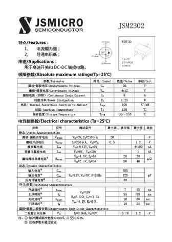
JSM2302 /Features 1 2 /Applications DC-DC /Absolute maximum ratings(Ta=25 ) /Parameter / Symbol /Value /Unit - /Drain-Source Voltage V 20 V DS - /Gate-Source Voltage V 12 V GS /C... See More ⇒
lpm2302b3f.pdf
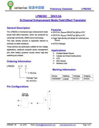
Preliminary Datasheet LPM2302 LPM2302 20V/3.5A N-Channel Enhancement Mode Field Effect Transistor General Description Features The LPM2302 is N-channel logic enhancement mode 20V/3.5A, RDS(ON)=50m (Typ.)@VGS=4.5V power field effect transistor, which are produced by 20V/3.0A, R =75m (Typ.)@V =2.5V DS(ON) GS using high cell density, DMOS trench technology. Sup... See More ⇒
lnsc2302.pdf
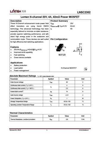
LNSC2302 Lonten N-channel 20V, 4A, 42m Power MOSFET Description Product Summary These N-Channel enhancement mode power field VDSS 20V effect transistors are using trench DMOS RDS(on).max@ VGS=4.5V 42m technology. This advanced technology has been ID 4A especially tailored to minimize on-state resistance, provide superior switching performance, and with stand high energy puls... See More ⇒
si2302s.pdf
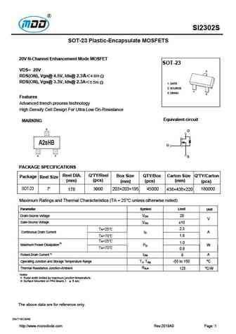
SI2302S SOT-23 Plastic-Encapsulate MOSFETS 20V N-Channel Enhancement Mode MOSFET SOT-23 VDS= 20V 3 RDS(ON), Vgs@ 4.5V, Ids@ 2.3A 4 8m RDS(ON), Vgs@ 3.3V, Ids@ 2.3A 5 5m 1. GATE 2. SOURCE 1 3. DRAIN 2 Features Advanced trench process technology High Density Cell Design For Ultra Low On-Resistance Equivalent circuit MARKING D A2sHB G S PACKAGE SPE... See More ⇒
si2302.pdf
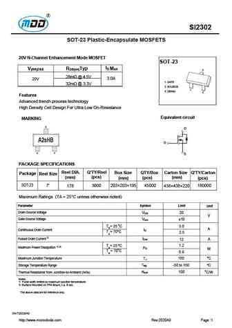
SI2302 SOT-23 Plastic-Encapsulate MOSFETS 20V N-Channel Enhancement Mode MOSFET SOT-23 ID Max V(BR)DSS RDS(on)Typ 3 28m @ 4.5V 3.0A 20V 1. GATE 32m @ 3.3V 2. SOURCE 1 3. DRAIN 2 Features Advanced trench process technology High Density Cell Design For Ultra Low On-Resistance Equivalent circuit MARKING D A2sHB G S PACKAGE SPECIFICATIONS Reel DIA. Q'TY/Ree... See More ⇒
si2302ai-ms.pdf
www.msksemi.com SI2302AI-MS Semiconductor Compiance General Features V = 20V,I = 3 A DS D R ... See More ⇒
mem2302x.pdf
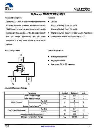
MEM2302 N-Channel MOSFET MEM2302X General Description Features MEM2302XG Series N-channel enhancement mode 20V/3A field-effect transistor ,produced with high cell density RDS(ON) =29m @ VGS=4.5V, ID=3A DMOS trench technology, which is especially used to RDS(ON) =36m @ VGS=2.5V, ID=2A minimize on-state resistance. This device particularly High Density Cell Design For Ultra... See More ⇒
mem2302xg-n.pdf
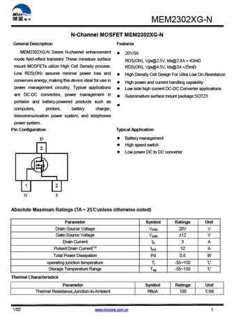
MEM2302XG-N N-Channel MOSFET MEM2302XG-N General Description Features MEM2302XG-N Series N-channel enhancement 20V/3A mode field-effect transistor These miniature surface RDS(ON), Vgs@2.5V, Ids@2.8A = 42m mount MOSFETs utilize High Cell Density process. RDS(ON), Vgs@4.5V, Ids@3A =35m Low RDS(ON) assures minimal power loss and High Density Cell Design For Ultra L... See More ⇒
mem2302m3.pdf
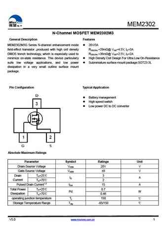
MEM2302 N-Channel MOSFET MEM2302M3 General Description Features MEM2302M3G Series N-channel enhancement mode 20V/3A field-effect transistor ,produced with high cell density RDS(ON) =29m @ VGS=4.5V, ID=3A DMOS trench technology, which is especially used to RDS(ON) =36m @ VGS=2.5V, ID=2A minimize on-state resistance. This device particularly High Density Cell Design For Ultra Low ... See More ⇒
si2302.pdf

SOT-23 Plastic-Encapsulate MOSFETS SI2302 SI2302 N-Channel 20-V(D-S) MOSFET V(BR)DSS RDS(on)MAX ID SOT-23 0.045 @ 4.5V 3 20V 3A 1.GATE 0.055 @ 2.5V 2.SOURCE 3.DRAIN 1 2 General FEATURE TrenchFET Power MOSFET Lead free product is acquired MARKING Equivalent Circuit Surface mount package A2sHB w APPLICATION Load Switch for Portable Devices DC/DC Converter *... See More ⇒
si2302a.pdf
SOT-23 Plastic-Encapsulate MOSFETS SI2302A N-Channel 20-V(D-S) MOSFET SI2302A V(BR)DSS RDS(on)MAX ID SOT-23 0.040 @ 4.5V 3 20V 3A 1.GATE 0.050 @ 2.5V 2.SOURCE 3.DRAIN 1 2 General FEATURE TrenchFET Power MOSFET Lead free product is acquired Equivalent Circuit MARKING Surface mount package A2 w APPLICATION Load Switch for Portable Devices DC/DC Converter *... See More ⇒
ks2302aa.pdf
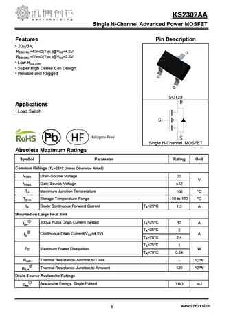
KS2302AA Single N-Channel Advanced Power MOSFET Features Pin Description 20V/3A, RDS (ON) =43m (Typ.)@VGS=4.5V D RDS (ON) =55m (Typ.)@VGS=2.5V Low RDS (ON) Super High Dense Cell Design Reliable and Rugged G S SOT23 D Applications Load Switch G S Single N-Channel MOSFET Absolute Maximum Ratings Symbol Parameter Rating Unit Common Ratings (TA=25 C U... See More ⇒
pjm2302nsa.pdf
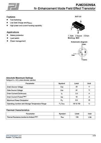
PJM2302NSA N- Enhancement Mode Field Effect Transistor SOT-23 Features Fast Switching Low Gate Charge and R DS(on) High power and current handing capability Applications Battery protection 1. Gate 2.Source 3.Drain Marking M22 Load switch Power management Schematic diagram 3Drain 1 Gate 2 Source Absolute Maximum Ratings Ratings at TC = 25 unless... See More ⇒
pjm2302nsa-s.pdf
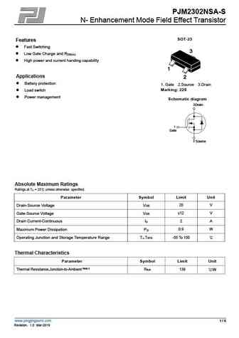
PJM2302NSA-S N- Enhancement Mode Field Effect Transistor SOT-23 Features Fast Switching Low Gate Charge and R DS(on) High power and current handing capability Applications Battery protection 1. Gate 2.Source 3.Drain Marking 22S Load switch Power management Schematic diagram 3Drain 1 Gate 2 Source Absolute Maximum Ratings Ratings at TC = 25 unle... See More ⇒
2302p.pdf
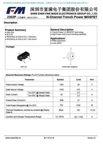
FM , FM WWW.SZLCSC.COM, SHEN ZHEN FINE MADE ELECTRONICS GROUP CO., LTD. 2302P S&CIC1975 N-Channel Trench Power MOSFET Description General Description Product Summary Trench Power LV MOSFET tech... See More ⇒
si2302.pdf
SI2302 20V N-Channel Enhancement Mode MOSFET VDS= 20V RDS(ON), Vgs@ 4.5V, Ids@ 4A 45m RDS(ON), Vgs@ 2.5V, Ids@ 3.5A 59m Features Advanced trench process technology High Density Cell Design For Ultra Low On-Resistance Package Dimensions D SOT-23 G S Millimeter Millimeter REF. REF. Min. Max. Min. Max. A 2.80 3.00 G 1.80 2.00 B 2.30 2.50 H 0.90 1.1 C 1.20 1.4... See More ⇒
sk2302aa.pdf
SK2302AA SOT-23 Plastic-Encapsulate Transistors FEATURES Trench FET Power MOSFET MARKING A2SHB MAXIMUM RATINGS (TA=25 unless otherwise noted) Symbol Parameter Value Units VDS Drain-Source voltage 20 V VGS Gate-Source voltage 10 V ID Drain current 2.9 A PD Power Dissipation 1 W Tj Junction Temperature 150 Tstg Storage Temperature -55-150 ELECTRICAL CHARACTER... See More ⇒
sk2302aat.pdf
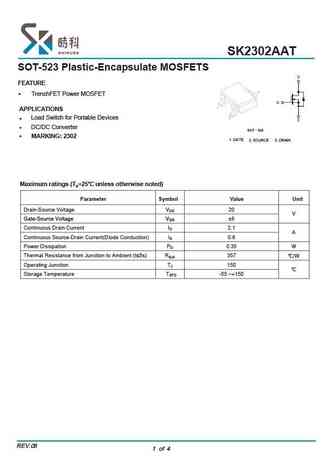
SK2302AAT SOT-523 Plastic-Encapsulate MOSFETS FEATURE TrenchFET Power MOSFET APPLICATIONS Load Switch for Portable Devices DC/DC Converter SOT 523 MARKING 2302 1. GATE 2. SOURCE 3. DRAIN Maximum ratings (T a =25 unless otherwise noted) Parameter Symbol Value Unit Drain-Source Voltage VDS 20 V Gate-Source Voltage VGS 8 Continuous Drain Current ID 2.1 ... See More ⇒
wtm2302.pdf
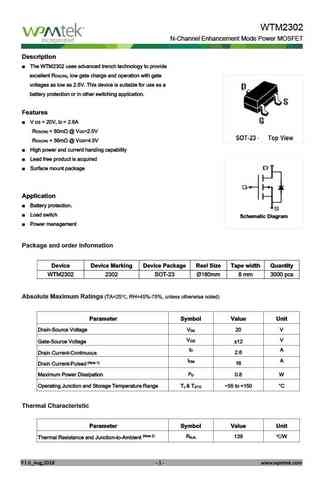
WTM2302 N-Channel Enhancement Mode Power MOSFET Description The WTM2302 uses advanced trench technology to provide excellent R , low gate charge and operation with gate DS(ON) voltages as low as 2.5V. This device is suitable for use as a battery protection or in other switching application. Features V DS = 20V, lD = 2.6A R ... See More ⇒
si2302.pdf
SI2302 N-Channel 20-V(D-S) MOSFET V(BR)DSS RDS(on)MAX ID SOT-23 0.050 @ 4.5V 3 20V 3A 1.GATE 0.065 @ 2.5V 2.SOURCE 3.DRAIN 1 2 General FEATURE TrenchFET Power MOSFET Lead free product is acquired MARKING Equivalent Circuit Surface mount package A2Shb APPLICATION Load Switch for Portable Devices DC/DC Converter Maximum ratings (Ta=25 unless otherwise not... See More ⇒
si2302.pdf
SHENZHEN LONG JING MICRO-ELECTRONICS CO., LTD. SOT-23 Plastic-Encapsulate MOSFETS SI2302 N-Channel 20V(D-S) MOSFET Features V = 20V, I = 2.5A DS D R ... See More ⇒
tf2302a.pdf

SHENZHEN TUOFENG SEMICONDUCTOR TECHNOLOGY CO.,LTD SOT-23 Plastic-Encapsulate MOSFETS TF2302A N-Channel 20-V(D-S) MOSFET TF2302A V(BR)DSS RDS(on)MAX ID SOT-23 0.040 @ 4.5V 3 20V 3A 1.GATE 0.050 @ 2.5V 2.SOURCE 3.DRAIN 1 2 General FEATURE TrenchFET Power MOSFET Lead free product is acquired Equivalent Circuit MARKING Surface mount package A2 w APPLICATION Load... See More ⇒
tf2302.pdf
SHENZHEN TUOFENG SEMICONDUCTOR TECHNOLOGY CO.,LTD SOT-23 Plastic-Encapsulate MOSFETS TF2302 TF2302 N-Channel 20-V(D-S) MOSFET V(BR)DSS RDS(on)MAX ID SOT-23 0.045 @ 4.5V 3 20V 3A 1.GATE 0.055 @ 2.5V 2.SOURCE 3.DRAIN 1 2 General FEATURE TrenchFET Power MOSFET Lead free product is acquired MARKING Equivalent Circuit Surface mount package A2sHB w APPLICATION Load... See More ⇒
si2302.pdf
SI2305 SI2301 SI2302 SI2302 SI2302 SI2302 SI2302 SI2301 Equivalent Circuit MARKING 3400 R A2SHB 3400 1.GATE 2.SOURCE 3.DRAIN ... See More ⇒
wst2302.pdf
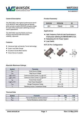
WST2302 N-Ch MOSFET General Description Product Summery The WST2302 is the highest performance trench BVDSS RDSON ID N-Ch MOSFET with extreme high cell density , which provide excellent RDSON and gate charge 20V 70m 3.0A for most of the small power switching and load switch applications. Applications The WST2302 meet the RoHS and Green Product requirement with full functio... See More ⇒
se2302.pdf
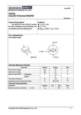
SHANGHAI July 2008 MICROELECTRONICS CO., LTD. SE2302 2.4A,20V N-Channel MOSFET Revision A General Description Features The MOSFETs from SINO-IC provide VDS (V) = 20V the best combination of fast switching, low ID = 2.4A on-resistance and cost-effectiveness. RDS(ON) ... See More ⇒
se2302u.pdf
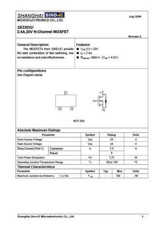
SHANGHAI July 2008 MICROELECTRONICS CO., LTD. SE2302U 2.4A,20V N-Channel MOSFET Revision A General Description Features The MOSFETs from SINO-IC provide VDS (V) = 20V the best combination of fast switching, low ID = 2.4A on-resistance and cost-effectiveness. RDS(ON) ... See More ⇒
sm2302.pdf
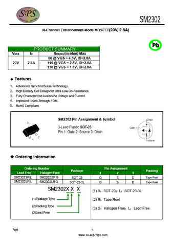
SM2302 N-Channel Enhancement-Mode MOSFET(20V, 2.8A) Pb PRODUCT SUMMARY VDSS ID RDS(on) (m-ohm) Max 60 @ VGS = 4.5V, ID=2.8A 20V 2.8A 115 @ VGS = 2.5V, ID=2.0A 130 @ VGS = 1.8V, ID=2.0A Features 1 Advanced Trench Process Technology. 2 High Density Cell Design for Ultra Low On-Resistance. 3 Fully Characterized Avalanche Voltage and Current. 4 Improved Shoot... See More ⇒
spn2302s23r.pdf
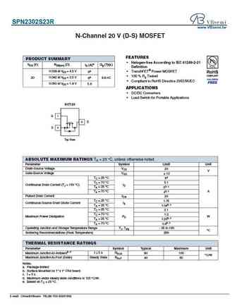
SPN2302S23R www.VBsemi.tw N-Channel 20 V (D-S) MOSFET FEATURES PRODUCT SUMMARY Halogen-free According to IEC 61249-2-21 VDS (V) RDS(on) ( ) ID (A)e Qg (Typ.) Definition 0.028 at VGS = 4.5 V TrenchFET Power MOSFET 6a 100 % Rg Tested 20 0.042 at VGS = 2.5 V 6a 8.8 nC Compliant to RoHS Directive 2002/95/EC 0.050 at VGS = 1.8 V 5.6 APPLICATIONS DC/... See More ⇒
ces2302.pdf
CES2302 www.VBsemi.tw N-Channel 20 V (D-S) MOSFET FEATURES PRODUCT SUMMARY Halogen-free According to IEC 61249-2-21 VDS (V) RDS(on) ( ) ID (A)e Qg (Typ.) Definition 0.028 at VGS = 4.5 V TrenchFET Power MOSFET 6a 100 % Rg Tested 20 0.042 at VGS = 2.5 V 6a 8.8 nC Compliant to RoHS Directive 2002/95/EC 0.050 at VGS = 1.8 V 5.6 APPLICATIONS DC/DC C... See More ⇒
st2302.pdf

ST2302 www.VBsemi.tw N-Channel 20 V (D-S) MOSFET FEATURES PRODUCT SUMMARY Halogen-free According to IEC 61249-2-21 VDS (V) RDS(on) ( ) ID (A)e Qg (Typ.) Definition 0.028 at VGS = 4.5 V TrenchFET Power MOSFET 6a 100 % Rg Tested 20 0.042 at VGS = 2.5 V 6a 8.8 nC Compliant to RoHS Directive 2002/95/EC 0.050 at VGS = 1.8 V 5.6 APPLICATIONS DC/DC Co... See More ⇒
si2302ds-t1-ge3.pdf
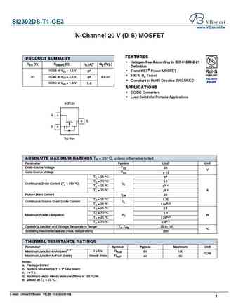
SI2302DS-T1-GE3 www.VBsemi.tw N-Channel 20 V (D-S) MOSFET FEATURES PRODUCT SUMMARY Halogen-free According to IEC 61249-2-21 VDS (V) RDS(on) ( ) ID (A)e Qg (Typ.) Definition 0.028 at VGS = 4.5 V TrenchFET Power MOSFET 6a 100 % Rg Tested 20 0.042 at VGS = 2.5 V 6a 8.8 nC Compliant to RoHS Directive 2002/95/EC 0.050 at VGS = 1.8 V 5.6 APPLICATIONS DC/D... See More ⇒
si2302ads-t1.pdf

SI2302ADS-T1 www.VBsemi.tw N-Channel 20 V (D-S) MOSFET FEATURES PRODUCT SUMMARY Halogen-free According to IEC 61249-2-21 VDS (V) RDS(on) ( ) ID (A)e Qg (Typ.) Definition 0.028 at VGS = 4.5 V TrenchFET Power MOSFET 6a 100 % Rg Tested 20 0.042 at VGS = 2.5 V 6a 8.8 nC Compliant to RoHS Directive 2002/95/EC 0.050 at VGS = 1.8 V 5.6 APPLICATIONS DC/DC C... See More ⇒
ut2302g-ae3.pdf

UT2302G-AE3 www.VBsemi.tw N-Channel 20 V (D-S) MOSFET FEATURES PRODUCT SUMMARY Halogen-free According to IEC 61249-2-21 VDS (V) RDS(on) ( ) ID (A)e Qg (Typ.) Definition 0.028 at VGS = 4.5 V TrenchFET Power MOSFET 6a 100 % Rg Tested 20 0.042 at VGS = 2.5 V 6a 8.8 nC Compliant to RoHS Directive 2002/95/EC 0.050 at VGS = 1.8 V 5.6 APPLICATIONS DC/... See More ⇒
mem2302.pdf
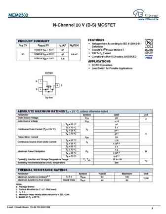
MEM2302 www.VBsemi.tw N-Channel 20 V (D-S) MOSFET FEATURES PRODUCT SUMMARY Halogen-free According to IEC 61249-2-21 VDS (V) RDS(on) ( ) ID (A)e Qg (Typ.) Definition 0.028 at VGS = 4.5 V TrenchFET Power MOSFET 6a 100 % Rg Tested 20 0.042 at VGS = 2.5 V 6a 8.8 nC Compliant to RoHS Directive 2002/95/EC 0.050 at VGS = 1.8 V 5.6 APPLICATIONS DC/DC Conver... See More ⇒
ut2302l-ae3.pdf
UT2302L-AE3 www.VBsemi.tw N-Channel 20 V (D-S) MOSFET FEATURES PRODUCT SUMMARY Halogen-free According to IEC 61249-2-21 VDS (V) RDS(on) ( ) ID (A)e Qg (Typ.) Definition 0.028 at VGS = 4.5 V TrenchFET Power MOSFET 6a 100 % Rg Tested 20 0.042 at VGS = 2.5 V 6a 8.8 nC Compliant to RoHS Directive 2002/95/EC 0.050 at VGS = 1.8 V 5.6 APPLICATIONS DC/... See More ⇒
st2302msrg.pdf
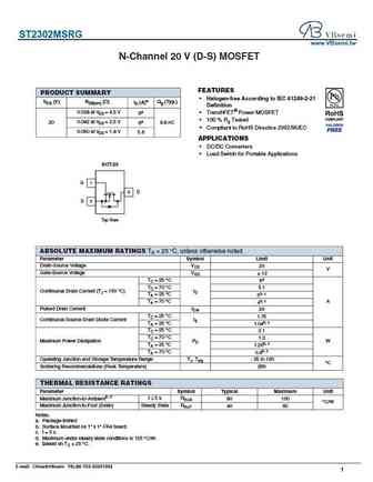
ST2302MSRG www.VBsemi.tw N-Channel 20 V (D-S) MOSFET FEATURES PRODUCT SUMMARY Halogen-free According to IEC 61249-2-21 VDS (V) RDS(on) ( ) ID (A)e Qg (Typ.) Definition 0.028 at VGS = 4.5 V TrenchFET Power MOSFET 6a 100 % Rg Tested 20 0.042 at VGS = 2.5 V 6a 8.8 nC Compliant to RoHS Directive 2002/95/EC 0.050 at VGS = 1.8 V 5.6 APPLICATIONS DC/D... See More ⇒
am2302n.pdf

AM2302N www.VBsemi.tw N-Channel 20 V (D-S) MOSFET FEATURES PRODUCT SUMMARY Halogen-free According to IEC 61249-2-21 VDS (V) RDS(on) ( ) ID (A)e Qg (Typ.) Definition 0.028 at VGS = 4.5 V TrenchFET Power MOSFET 6a 100 % Rg Tested 20 0.042 at VGS = 2.5 V 6a 8.8 nC Compliant to RoHS Directive 2002/95/EC 0.050 at VGS = 1.8 V 5.6 APPLICATIONS DC/DC Conver... See More ⇒
si2302cds-t1-ge3.pdf

SI2302CDS-T1-GE3 www.VBsemi.tw N-Channel 20 V (D-S) MOSFET FEATURES PRODUCT SUMMARY Halogen-free According to IEC 61249-2-21 VDS (V) RDS(on) ( ) ID (A)e Qg (Typ.) Definition 0.028 at VGS = 4.5 V TrenchFET Power MOSFET 6a 100 % Rg Tested 20 0.042 at VGS = 2.5 V 6a 8.8 nC Compliant to RoHS Directive 2002/95/EC 0.050 at VGS = 1.8 V 5.6 APPLICATIONS DC/... See More ⇒
yjl2302b.pdf
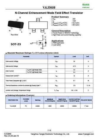
RoHS COMPLIANT YJL2302B N-Channel Enhancement Mode Field Effect Transistor Product Summary V 20V DS I 3.0A D R ( at V =4.5V) 52 mohm DS(ON) GS R ( at V =2.5V) 80 mohm DS(ON) GS General Description Trench Power LV MOSFET technology High Power and current handing capability Applications PWM application Load switch Absolute Ma... See More ⇒
yjl2302a.pdf

RoHS COMPLIANT YJL2302A N-Channel Enhancement Mode Field Effect Transistor Product Summary V 20V DS I 4.3A D R ( at V =4.5V) 27 mohm DS(ON) GS R ( at V =2.5V) 37 mohm DS(ON) GS General Description Trench Power LV MOSFET technology High Power and current handing capability Applications PWM application Load switch Absolute M... See More ⇒
ttx2302a.pdf
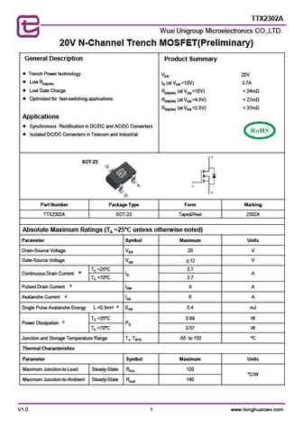
TTX2302A Wuxi Unigroup Microelectronics CO.,LTD. 20V N-Channel Trench MOSFET(Preliminary) General Description Product Summary Trench Power technology VDS 20V Low RDS(ON) ID (at VGS =10V) 3.7A Low Gate Charge RDS(ON) (at VGS =10V) ... See More ⇒
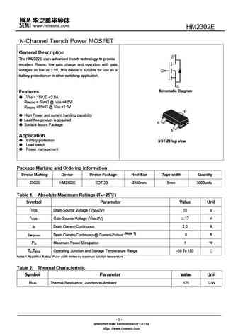
ttx2302.pdf
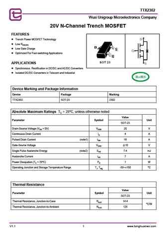
TTX2302 Wuxi Unigroup Microelectronics Company Wuxi Unigroup Microelectronics Company 20V N-Channel Trench MOSFET FEATURES Trench Power MOSFET Technology Low RDS(ON) Low Gate Charge Optimized For Fast-switching Applications APPLICATIONS Synchronous Rectification in DC/DC and AC/DC Converters Isolated DC/DC Converters in Telecom and Industrial Device Marking a... See More ⇒
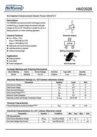
hm2302.pdf

HM2302 N-Channel Enhancement Mode Power MOSFET DESCRIPTION D The HM2302 uses advanced trench technology to provide excellent RDS(ON), low gate charge and operation with gate G voltages as low as 2.5V. This device is suitable for use as a Battery protection or in other Switching application. S Schematic diagram GENERAL FEATURES VDS = 20V,ID = 2.9A D 3 RDS(ON) ... See More ⇒
hm2302bwsr.pdf
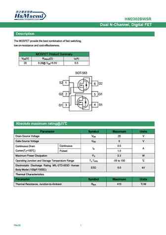
Description The MOSFET provide the best combination of fast switching, low on-resistance and cost-effectiveness. MOSFET Product Summary VDS(V) RDS(on)( ) ID(A) 20 0.29@ VGS=4.5V 0.5 SOT-563 S2 1 D2 6 G2 2 G1 5 4 S1 3 D1 Absolute maximum rating@25 Parameter Symbol Maximum Units Drain-Source Voltage ... See More ⇒
hm2302kr.pdf
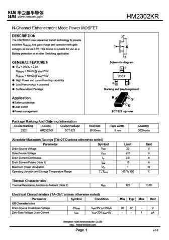
HM2302KR N-Channel Enhancement Mode Power MOSFET DESCRIPTION D The HM2302KR uses advanced trench technology to provide excellent RDS(ON), low gate charge and operation with gate G voltages as low as 2.5V. This device is suitable for use as a Battery protection or in other Switching application. S Schematic diagram GENERAL FEATURES VDS = 20V,ID = 2.9A D 3 RDS(ON) ... See More ⇒
hm2302f.pdf

HM2302F N-Channel Enhancement Mode Power MOSFET Description The HM2302F uses advanced trench technology to provide excellent RDS(ON), low gate charge and operation with gate voltages as low as 2.5V. This device is suitable for use as a Battery protection or in other Switching application. Schematic diagram General Features VDS = 20V,ID = 2.8A RDS(ON) ... See More ⇒
hm2302dr.pdf
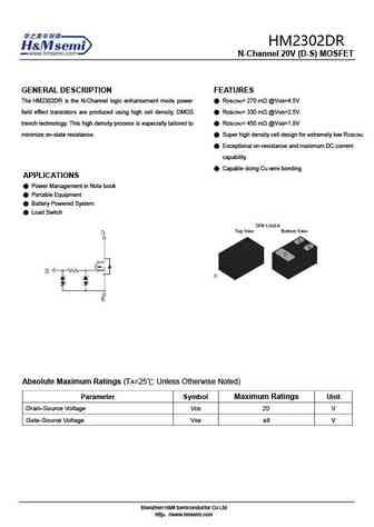
GENERAL DESCRIPTION FEATURES The HM2302DR is the N-Channel logic enhancement mode power RDS(ON)= 270 m @VGS=4.5V field effect transistors are produced using high cell density, DMOS RDS(ON)= 330 m @VGS=2.5V trench technology. This high density process is especially tailored to RDS(ON)= 450 m @VGS=1.8V minimize on-state resistan... See More ⇒
hm2302bwkr.pdf
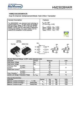
HM2302BWKR Dual N-Channel Enhancement Mode Field Effect Transistor General Description Features The HM2302BWKR uses advanced trench technology to VDS (V) = 20V ID = 0.9 A (VGS = 4.5V) excellent RDS(ON), low gate charge and operation voltages as low as 1.8V, in the small SOT363 RDS(ON) ... See More ⇒
hm2302bjr.pdf
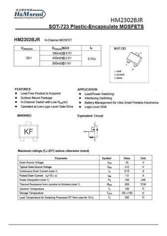
J HM2302BJR SOT-723 Plastic-Encapsulate MOSFETS HM2302BJR N-Channel MOSFET ID V(BR)DSS RDS(on)MAX SOT-723 380m @ 4.5V 20V 450m @2.5V 0.75A 800m @1.8V 1. GATE 2. SOURCE 3. DRAIN FEATURES APPLICATION Lead Free Product is Acquired Load/Power Switching Surface Mount Package Interfacing Switching N-Channel Switch with Low RDS(on) Battery Manage... See More ⇒
hm2302b.pdf
HM2302B N-Channel Enhancement Mode Power MOSFET Description The HM2302B uses advanced trench technology to provide excellent RDS(ON), low gate charge and operation with gate voltages as low as 2.5V. This device is suitable for use as a Battery protection or in other Switching application. Schematic diagram General Features VDS = 20V,ID = 2.5A RDS(ON) ... See More ⇒
hm2302e.pdf
HM2302E N-Channel Trench Power MOSFET General Description The HM2302E uses advanced trench technology to provide excellent R , low gate charge and operation with gate DS(ON) voltages as low as 2.5V. This device is suitable for use as a battery protection or in other switching application. Schematic Diagram Features VDS = 15V,ID =2.0A R ... See More ⇒
hm2302d.pdf
GENERAL DESCRIPTION FEATURES The HM2302D is the N-Channel logic enhancement mode power RDS(ON)= 270 m @VGS=4.5V field effect transistors are produced using high cell density, DMOS RDS(ON)= 330 m @VGS=2.5V trench technology. This high density process is especially tailored to RDS(ON)= 450 m @VGS=1.8V minimize on-state resistance... See More ⇒
hnm2302.pdf
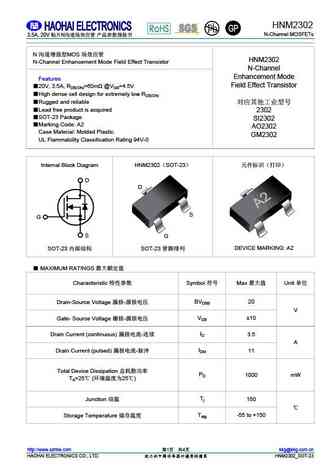
HNM2302 N-Channel MOSFETs 3.5A, 20V N N MOS HNM2302 N-Channel Enhancement Mode Field Effect Transistor N-Channel Enhancement Mode Features Field Effect Transistor 20V, 3.5A, RDS(ON)=60m @VGS=4.5V High dense cell design for extremely low RDS(ON) Rugged and reliable ... See More ⇒
h2302.pdf
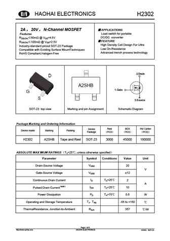
HAOHAI ELECTRONICS H2302 2A 20V N-Channel MOSFET APPLICATIONS Load switch for portable Features DC/DC converter RDS(ON) 60m @ VGS=4.5V FEATURE RDS(ON) 100m @ VGS=2.5V High Density Cell Design For Ultra Industry-standard pinout SOT-23 Package Low On-Resistance Compatible with Existing Surface MountTechniques ... See More ⇒
h2302a.pdf
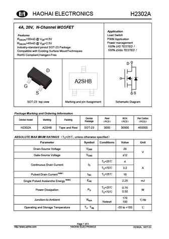
HAOHAI ELECTRONICS H2302A 4A, 20V, N-Channel MOSFET Application Load Switch Features PWM Application RDS(ON)... See More ⇒
hnm2302alb.pdf
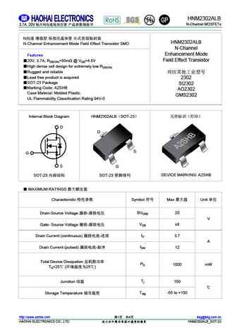
HNM2302ALB N-Channel MOSFETs 3.7A, 20V N N HNM2302ALB N-Channel Enhancement Mode Field Effect Transistor SMD N-Channel Enhancement Mode Features Field Effect Transistor 20V, 3.7A, RDS(ON)=50m @ VGS=4.5V High dense cell design for extremely low RDS(ON) ... See More ⇒
ap2302ai.pdf
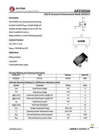
AP2302AI 20V N-Channel Enhancement Mode MOSFET Description The AP2302AI uses advanced trench technology to provide excellent R , low gate charge and DS(ON) operation with gate voltages as low as 2.5V. This device is suitable for use as a Battery protection or in other Switching application. General Features V = 20V I =3.2A DS D R ... See More ⇒
ap2302ci.pdf
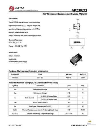
AP2302CI 20V N-Channel Enhancement Mode MOSFET Description The AP2302CI uses advanced trench technology to provide excellent R , low gate charge and DS(ON) operation with gate voltages as low as 2.5V. This device is suitable for use as a Battery protection or in other Switching application. General Features V = 20V I =2.3A DS D R ... See More ⇒
Detailed specifications: SSS7N60 , SSS8N60 , 1002 , 1115 , 1515 , G1601 , 2300 , 2301 , AOD4184A , 3035 , 3400 , 3401 , 3415 , 6616 , 6703 , 6760 , 7080 .
History: 1002
Keywords - 2302 MOSFET specs
2302 cross reference
2302 equivalent finder
2302 pdf lookup
2302 substitution
2302 replacement
Can't find your MOSFET? Learn how to find a substitute transistor by analyzing voltage, current and package compatibility
History: 1002
🌐 : EN ES РУ

LIST
Last Update
MOSFET: ASB80R750E | ASB70R380E | ASB65R300E | ASB65R220E | ASB65R120EFD | ASB60R150E | ASA80R900E | ASA80R750E | ASA80R290E | ASA70R950E
Popular searches
2n3054 transistor equivalent | 2n554 | 2sa1011 | 2sa1283 | 2sb646 | 2sc1885 datasheet | 2sc2580 | 2sc710