10N03 Specs and Replacement
Type Designator: 10N03
Type of Transistor: MOSFET
Type of Control Channel: N-Channel
Absolute Maximum Ratings
Pd ⓘ
- Maximum Power Dissipation: 2.5 W
|Vds|ⓘ - Maximum Drain-Source Voltage: 30 V
|Vgs|ⓘ - Maximum Gate-Source Voltage: 20 V
|Id| ⓘ - Maximum Drain Current: 10 A
Tj ⓘ - Maximum Junction Temperature: 150 °C
Electrical Characteristics
Cossⓘ -
Output Capacitance: 300 pF
RDSonⓘ - Maximum Drain-Source On-State Resistance: 0.0135 Ohm
Package: SOP8
- MOSFET ⓘ Cross-Reference Search
10N03 datasheet
..1. Size:2459K goford
10n03.pdf 
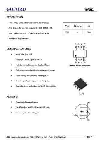
GOFORD 10N03 DESCRIPTION The 10N03 uses advanced trench technology VDS RDS(ON) ID And design to provide excellent RDS (ON ) with 30V -- 10A Low gate charge . It can be used in a wide Vanety of applications . GENERAL FEATURES VDS = 30 V, ID = 10 A RDS(ON) ... See More ⇒
0.1. Size:2101K 1
cjac110n03.pdf
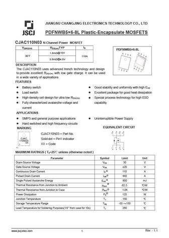
JIANGSU CHANGJING ELECTRONICS TECHNOLOGY CO., LTD PDFN 5 6-8L Plastic-Encapsulate MOSFETS CJAC110N03 N-Channel Power MOSFET ID V(BR)DSS RDS(on)TYP PDFN 5 6-8L 1.8m @10V 30 V 110A 3.5m @4.5V DESCRIPTION FEATURES... See More ⇒
0.2. Size:201K motorola
mmsf10n03z.pdf
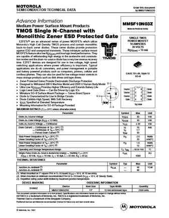
MOTOROLA Order this document SEMICONDUCTOR TECHNICAL DATA by MMSF10N03Z/D Advance Information MMSF10N03Z Medium Power Surface Mount Products Motorola Preferred Device TMOS Single N-Channel with Monolithic Zener ESD Protected Gate SINGLE TMOS POWER MOSFET EZFETs are an advanced series of power MOSFETs which utilize 10 AMPERES Motorola s High Cell Density TMOS process and conta... See More ⇒
0.3. Size:196K motorola
mmsf10n03zrev0.pdf

MOTOROLA Order this document SEMICONDUCTOR TECHNICAL DATA by MMSF10N03Z/D Advance Information MMSF10N03Z Medium Power Surface Mount Products Motorola Preferred Device TMOS Single N-Channel with Monolithic Zener ESD Protected Gate SINGLE TMOS POWER MOSFET EZFETs are an advanced series of power MOSFETs which utilize 10 AMPERES Motorola s High Cell Density TMOS process and conta... See More ⇒
0.4. Size:257K renesas
np110n03pug.pdf
To our customers, Old Company Name in Catalogs and Other Documents On April 1st, 2010, NEC Electronics Corporation merged with Renesas Technology Corporation, and Renesas Electronics Corporation took over all the business of both companies. Therefore, although the old company name remains in this document, it is a valid Renesas Electronics document. We appreciate your understanding. ... See More ⇒
0.5. Size:166K rohm
rsh110n03tb1.pdf
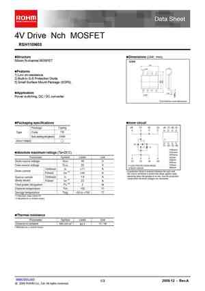
4V Drive Nch MOSFET RSH110N03 Structure Dimensions (Unit mm) Silicon N-channel MOSFET SOP8 Features 1) Low on-resistance. 2) Built-in G-S Protection Diode. 3) Small Surface Mount Package (SOP8). Application Power switching, DC / DC converter. Each lead has same dimensions Packaging specifications Inner circuit (8) (7) (6) (5) (8) (7) (6) (5) Package ... See More ⇒
0.6. Size:98K rohm
rrs110n03tb1.pdf
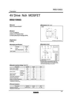
RRS110N03 Transistor 4V Drive Nch MOSFET RRS110N03 Structure Dimensions (Unit mm) Silicon N-channel MOSFET SOP8 Features 1) Low on-resistance. 2) Built-in G-S Protection Diode. 3) Small Surface Mount Package (SOP8). Applications Each lead has same dimensions Switching Equivalent circuit Packaging specifications (8) (7) (6) (5) (8) (7) (6) (5) Package Tapi... See More ⇒
0.7. Size:58K rohm
rss110n03fu6tb rss110n03tb.pdf
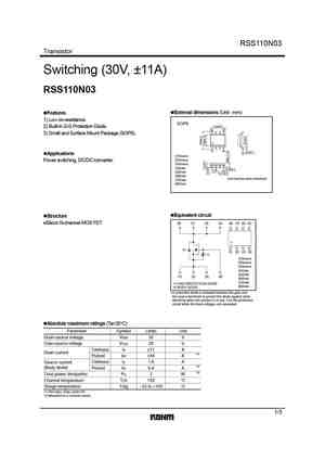
RSS110N03 Transistor Switching (30V, 11A) RSS110N03 External dimensions (Unit mm) Features 1) Low on-resistance. SOP8 5.0 0.2 2) Built-in G-S Protection Diode. 3) Small and Surface Mount Package (SOP8). 0.2 0.1 Applications (1)Source (2)Source Power switching, DC/DC converter. (3)Source (4)Gate 0.4 0.1 1.27 (5)Drain 0.1 (6)Drain Each lead has same dim... See More ⇒
0.8. Size:69K vishay
sum110n03-03p.pdf
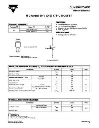
SUM110N03-03P Vishay Siliconix N-Channel 30-V (D-S) 175_C MOSFET FEATURES PRODUCT SUMMARY D TrenchFETr Power MOSFET D 175_C Junction Temperature V(BR)DSS (V) rDS(on) (W) ID (A)a D Optimized for Low-Side Synchronous Rectifier 0.0026 @ VGS = 10 V 110a D 100% Rg Tested 30 30 0.004 @ VGS = 4.5 V 110a APPLICATIONS D Desktop or Server CPU Core D TO-263 DRAIN connected to TAB G G D... See More ⇒
0.9. Size:74K vishay
sum110n03-04p.pdf
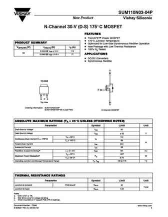
SUM110N03-04P New Product Vishay Siliconix N-Channel 30-V (D-S) 175_C MOSFET FEATURES D TrenchFETr Power MOSFET D 175_C Junction Temperature PRODUCT SUMMARY D Optimized for Low-Side Synchronous Rectifier Operation D New Package with Low Thermal Resistance V(BR)DSS (V) rDS(on) (W) ID (A) D 100% Rg Tested 0.0042 @ VGS = 10 V 110 30 30 0.0065 @ VGS = 4.5 V 77 APPLICATIONS D DC/DC C... See More ⇒
0.10. Size:671K infineon
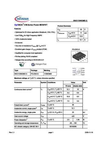
bso110n03ms.pdf
%" ! % %0 S 07DK >AI A@ D7E;EF3@57 0 D n) G S J57>>7@F 93F7 5 3D97 J BDA6G5F !* ( G D O D n) S , G3>;8;76 8AD 5A@EG?7D >7H7> 3BB>;53F;A@ S +4 8D77 B>3F;@9 - A#... See More ⇒
0.11. Size:553K infineon
bso110n03msg.pdf
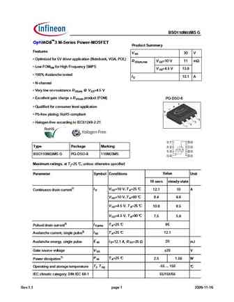
BSO110N03MS G OptiMOS 3 M-Series Power-MOSFET Product Summary Features V 30 V DS Optimized for 5V driver application (Notebook, VGA, POL) R V =10 V 11 m DS(on),max GS Low FOMSW for High Frequency SMPS V =4.5 V 13.9 GS 100% Avalanche tested I 12.1 A D N-channel Very low on-resistance R @ V =4.5 V DS(on) GS Excellent gate charge x R product (FOM) P... See More ⇒
0.12. Size:143K utc
ut110n03.pdf
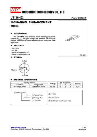
UNISONIC TECHNOLOGIES CO., LTD UT110N03 Power MOSFET N-CHANNEL ENHANCEMENT MODE DESCRIPTION The UT110N03 uses advanced trench technology to provide excellent RDS(ON), low gate charge and operation with low gate voltages. This device is suitable for use as a load switch or in PWM applications. FEATURES * VDS(V)=26V * ID=110A * RDS(ON) =4.8m @VGS=10 V * RDS(ON) =7.... See More ⇒
0.13. Size:75K secos
sse110n03-03p.pdf
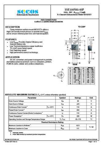
SSE110N03-03P 110A , 30V , RDS(ON) 2.5m N-Channel Enhancement Mode MOSFET Elektronische Bauelemente RoHS Compliant Product A suffix of -C specifies halogen and lead-free TO-220P DESCRIPTION These miniature surface mount MOSFETs utilize a D High Cell Density trench process to provide low RDS(on) C and to ensure minimal power loss and heat dissipatio... See More ⇒
0.14. Size:2101K jiangsu
cjac110n03.pdf
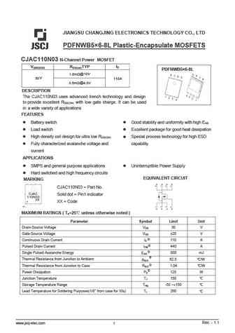
JIANGSU CHANGJING ELECTRONICS TECHNOLOGY CO., LTD PDFN 5 6-8L Plastic-Encapsulate MOSFETS CJAC110N03 N-Channel Power MOSFET ID V(BR)DSS RDS(on)TYP PDFN 5 6-8L 1.8m @10V 30 V 110A 3.5m @4.5V DESCRIPTION FEATURES... See More ⇒
0.15. Size:996K blue-rocket-elect
brcs010n03szc.pdf
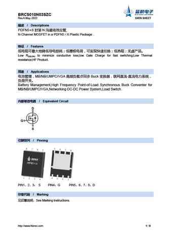
BRCS010N03SZC Rev.A May.-2022 DATA SHEET / Descriptions PDFN5 6 N N-Channel MOSFET in a PDFN5 6 Plastic Package . / Features Low RDS(ON) to minimize conductive loss;low Gate Charge for fast switching;Low Thermal resistance;... See More ⇒
0.16. Size:628K crhj
crtd110n03l.pdf
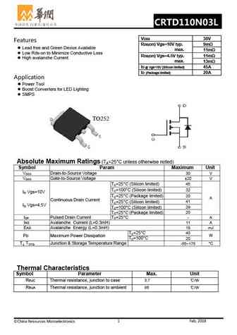
CRTD110N03L VDSS 30V Features RDS(on) Vgs=10V typ. 9m Lead free and Green Device Available max. 11m Low Rds-on to Minimize Conductive Loss RDS(on) Vgs=4.5V typ. 11m High avalanche Current max. 13m ID @ Vgs=10V (Silicon limited) 45A ID (Package limited) 20A Application Power Tool Boost Converters for LED Lighting SMPS TO252 Absolute Maximum Rat... See More ⇒
0.17. Size:1907K kexin
ndt110n03.pdf
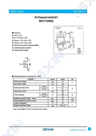
SMD Type MOSFET N-Channel MOSFET NDT110N03 TO-252 Unit mm +0.15 6.50-0.15 +0.1 2.30 -0.1 +0.2 Features 5.30-0.2 +0.8 0.50 -0.7 VDS (V) = 30V 4 ID = 110 A (VGS = 10V) RDS(ON) 4m (VGS = 10V) 0.127 +0.1 0.80-0.1 max RDS(ON) 6m (VGS = 4.5V) High Power and current handing capability + 0.1 Lead free product is acquired 2.3 0.60- 0... See More ⇒
0.18. Size:2698K maple semi
sla10n03t.pdf
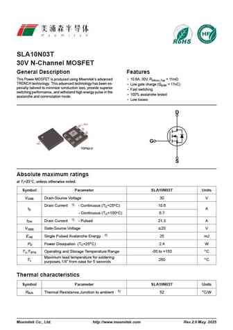
SLA10N03T 30V N-Channel MOSFET General Description Features This Power MOSFET is produced using Msemitek s advanced 10.6A, 30V, RDS(on),Typ = 11m TRENCH technology. This advanced technology has been es- Low gate charge (Qg,typ = 17nC) pecially tailored to minimize conduction loss, provide superior Fast switching switching performance, and withstand high energy pulse in t... See More ⇒
0.19. Size:753K semihow
hrlo110n03k.pdf
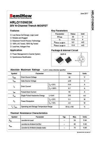
June 2017 HRLO110N03K 30V N-Channel Trench MOSFET Features Key Parameters Parameter Value Unit Low Dense Cell Design, Logic Level BVDSS 30 V Reliable and Rugged ID 13.8 A Advanced Trench Process Technology RDS(on), typ @10V 9.0 m 100% UIS Tested, 100% Rg Tested RDS(on), typ @4.5V 13.0 m Lead free, Halogen Free Application Package & Internal ... See More ⇒
0.20. Size:775K semihow
hrlf110n03k.pdf
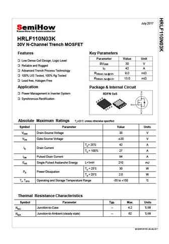
July 2017 HRLF110N03K 30V N-Channel Trench MOSFET Features Key Parameters Parameter Value Unit Low Dense Cell Design, Logic Level BVDSS 30 V Reliable and Rugged ID 42 A Advanced Trench Process Technology RDS(on), typ @10V 9.0 m 100% UIS Tested, 100% Rg Tested RDS(on), typ @4.5V 13.0 m Lead free, Halogen Free Application Package & Internal Ci... See More ⇒
0.21. Size:519K way-on
wmr10n03t1.pdf
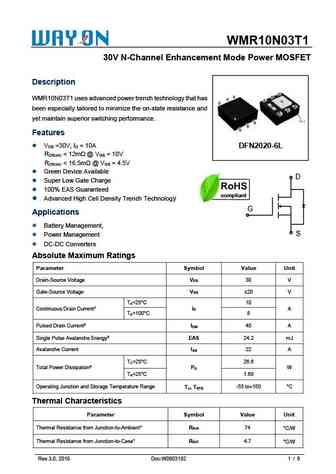
WMR10N03T1 30V N-Channel Enhancement Mode Power MOSFET Description WMR10N03T1 uses advanced power trench technology that has been especially tailored to minimize the on-state resistance and yet maintain superior switching performance. Features V =30V, I = 10A DS D DFN2020-6L R ... See More ⇒
0.22. Size:733K wuxi china
cs110n03a3.pdf
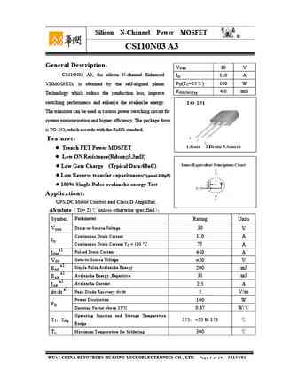
Silicon N-Channel Power MOSFET R CS110N03 A3 General Description VDSS 30 V CS110N03 A3, the silicon N-channel Enhanced ID 110 A PD(TC=25 ) 100 W VDMOSFETs, is obtained by the self-aligned planar RDS(ON)Typ 4.0 m Technology which reduce the conduction loss, improve switching performance and enhance the avalanche energy. The transistor can be used in various pow... See More ⇒
0.23. Size:659K convert
ctd10n033.pdf
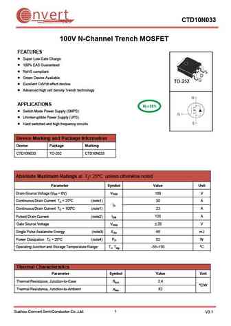
nvert CTD10N033 Suzhou Convert Semiconductor Co ., Ltd. 100V N-Channel Trench MOSFET FEATURES Super Low Gate Charge 100% EAS Guaranteed RoHS compliant Green Device Available Excellent CdV/dt effect decline Advanced high cell density Trench technology APPLICATIONS Switch Mode Power Supply (SMPS) Uninterruptible Power Supply (UPS) Hard switched an... See More ⇒
0.24. Size:547K cn hmsemi
hm110n03d.pdf
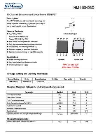
N-Channel Enhancement Mode Power MOSFET Description The HM110N03D uses advanced trench technology and design to provide excellent RDS(ON) with low gate charge. It can be used in a wide variety of applications. General Features VDS =30V,ID =110A Schematic Diagram RDS(ON) ... See More ⇒
0.25. Size:754K cn hmsemi
hm10n03d.pdf
N-Channel Enhancement Mode Power MOSFET Description The uses advanced trench technology and design to provide excellent RDS(ON) with low gate charge. It can be used in a wide variety of applications. General Features VDS =40V,ID =100A RDS(ON) ... See More ⇒
Detailed specifications: G23
, G11
, G16
, G17
, 03N06
, 05N06
, 100N03
, 100P03
, IRF630
, 110N10
, 11N10C
, 120N03
, 1402TR
, 1404TR
, 140N10
, ECYA
, G1002
.
Keywords - 10N03 MOSFET specs
10N03 cross reference
10N03 equivalent finder
10N03 pdf lookup
10N03 substitution
10N03 replacement
Step-by-step guide to finding a MOSFET replacement. Cross-reference parts and ensure compatibility for your repair or project.
