110N10 Specs and Replacement
Type Designator: 110N10
Type of Transistor: MOSFET
Type of Control Channel: N-Channel
Absolute Maximum Ratings
Pd ⓘ
- Maximum Power Dissipation: 220 W
|Vds|ⓘ - Maximum Drain-Source Voltage: 100 V
|Vgs|ⓘ - Maximum Gate-Source Voltage: 20 V
|Id| ⓘ - Maximum Drain Current: 110 A
Tj ⓘ - Maximum Junction Temperature: 175 °C
Electrical Characteristics
tr ⓘ - Rise Time: 24 nS
Cossⓘ -
Output Capacitance: 380 pF
RDSonⓘ - Maximum Drain-Source On-State Resistance: 0.009 Ohm
Package: TO220
- MOSFET ⓘ Cross-Reference Search
110N10 datasheet
..1. Size:2111K goford
110n10.pdf 
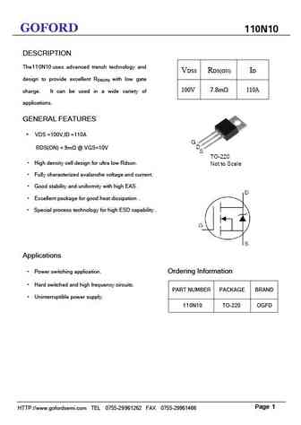
GOFORD 110N10 DESCRIPTION The110N10 uses advanced trench technology and VDSS RDS(ON) ID design to provide excellent R with low gate DS(ON) 100V 7.8m 110A charge. It can be used in a wide variety of applications. GENERAL FEATURES VDS =100V,ID =110A RDS(ON) ... See More ⇒
0.1. Size:1029K st
stl110n10f7.pdf
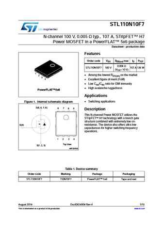
STL110N10F7 N-channel 100 V, 0.005 typ., 107 A, STripFET H7 Power MOSFET in a PowerFLAT 5x6 package Datasheet - production data Features Order code VDS RDS(on) max ID PTOT 0.006 STL110N10F7 100 V 107 A 136 W (VGS= 10 V) 1 2 Among the lowest RDS(on) on the market 3 4 Excellent figure of merit (FoM) Low Crss/Ciss ratio for EMI immunity High avalanche... See More ⇒
0.2. Size:858K st
sth110n10f7-2 sth110n10f7-6.pdf
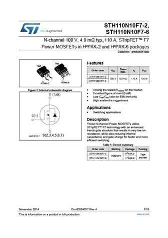
STH110N10F7-2, STH110N10F7-6 N-channel 100 V, 4.9 m typ.,110 A, STripFET F7 Power MOSFETs in H PAK-2 and H PAK-6 packages Datasheet - production data TAB Features TAB RDS(on) Order code VDS ID PTOT max. 7 2 STH110N10F7-2 3 1 100 V 6.5 m 110 A 150 W 1 STH110N10F7-6 H2PAK-6 H2PAK-2 Figure 1 Internal schematic diagram Among the lowest RDS(on) on the mar... See More ⇒
0.3. Size:1225K st
stf110n10f7 stp110n10f7.pdf
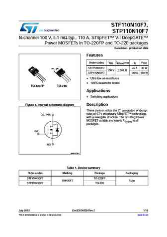
STF110N10F7, STP110N10F7 N-channel 100 V, 5.1 m typ., 110 A, STripFET VII DeepGATE Power MOSFETs in TO-220FP and TO-220 packages Datasheet - production data Features Order codes VDS RDS(on) max ID PTOT STF110N10F7 45 A 30 W TAB 100 V 0.007 STP110N10F7 110 A 150 W Ultra low on-resistance 3 3 2 2 1 1 100% avalanche tested TO-220FP TO-220 Applications Sw... See More ⇒
0.4. Size:164K vishay
sum110n10-09.pdf
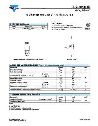
SUM110N10-09 Vishay Siliconix N-Channel 100 V (D-S) 175 C MOSFET FEATURES PRODUCT SUMMARY TrenchFET Power MOSFET VDS (V) RDS(on) ( )ID (A) New Package with Low Thermal Resistance 100 0.0095 at VGS = 10 V 110a 100 % Rg Tested D TO-263 G G D S Top View S Ordering Information SUM110N10-09-E3 (Lead (Pb)-free) N-Channel MOSFET ABSOLUTE MAXIMUM RATINGS TC = ... See More ⇒
0.5. Size:167K vishay
sqm110n10-09.pdf
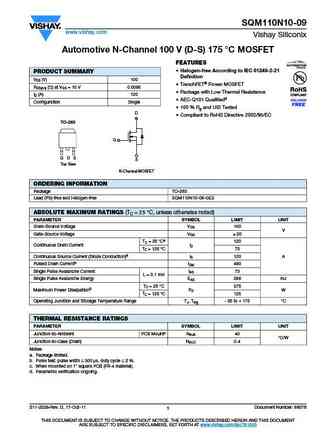
SQM110N10-09 www.vishay.com Vishay Siliconix Automotive N-Channel 100 V (D-S) 175 C MOSFET FEATURES Halogen-free According to IEC 61249-2-21 PRODUCT SUMMARY Definition VDS (V) 100 TrenchFET Power MOSFET RDS(on) ( ) at VGS = 10 V 0.0095 Package with Low Thermal Resistance ID (A) 120 AEC-Q101 Qualifiedd Configuration Single 100 % Rg and UIS Tested D ... See More ⇒
0.6. Size:170K ixys
ixtq110n10p ixtt110n10p.pdf
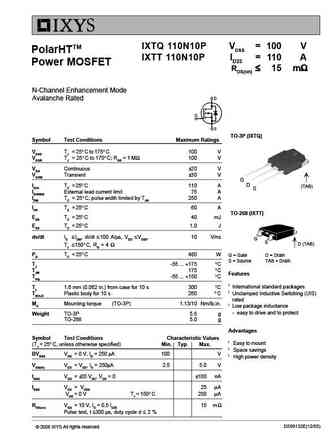
IXTQ 110N10P VDSS = 100 V PolarHTTM IXTT 110N10P ID25 = 110 A Power MOSFET RDS(on) 15 m N-Channel Enhancement Mode Avalanche Rated TO-3P (IXTQ) Symbol Test Conditions Maximum Ratings VDSS TJ = 25 C to 175 C 100 V VDGR TJ = 25 C to 175 C; RGS = 1 M 100 V VGS Continuous 20 V VGSM Transient 30 V G D ID25 TC = 25 C 110 A (T... See More ⇒
0.7. Size:309K ixys
ixfh110n10p ixfv110n10p.pdf
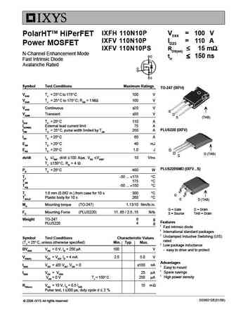
IXFH 110N10P VDSS = 100 V PolarHTTM HiPerFET IXFV 110N10P ID25 = 110 A Power MOSFET IXFV 110N10PS RDS(on) 15 m N-Channel Enhancement Mode trr 150 ns Fast Intrinsic Diode Avalanche Rated Symbol Test Conditions Maximum Ratings TO-247 (IXFH) VDSS TJ = 25 C to 175 C 100 V VDGR TJ = 25 C to 175 C; RGS = 1 M 100... See More ⇒
0.8. Size:230K ixys
ixfc110n10p.pdf
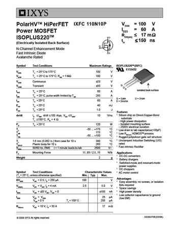
IXFC 110N10P VDSS = 100 V PolarHVTM HiPerFET ID25 = 60 A Power MOSFET RDS(on) 17 m ISOPLUS220TM trr 150 ns (Electrically Isolated Back Surface) N-Channel Enhancement Mode Fast Intrinsic Diode Avalanche Rated Symbol Test Conditions Maximum Ratings ISOPLUS220TM (IXFC) E153432 VDSS TJ = 25 C to 175 C 100 V VDGR TJ... See More ⇒
0.9. Size:705K matsuki electric
me110n10t me110n10f.pdf
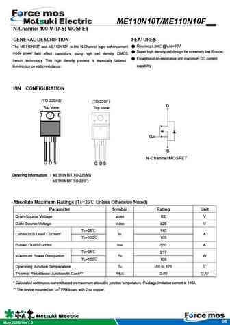
ME110N10T/ME110N10F N-Channel 100-V (D-S) MOSFET GENERAL DESCRIPTION FEATURES RDS(ON) 6.2m @VGS=10V The ME110N10T and ME110N10F is the N-Channel logic enhancement Super high density cell design for extremely low RDS(ON) mode power field effect transistors, using high cell density, DMOS Exceptional on-resistance and maximum DC current trench technology. This h... See More ⇒
0.10. Size:4212K first semi
fir110n10pg.pdf
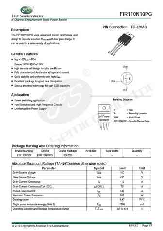
FIR110N10PG N-Channel Enhancement Mode Power Mosfet PIN Connection TO-220AB Description The FIR110N10PG uses advanced trench technology and design to provide excellent RDS(ON) with low gate charge. It can be used in a wide variety of applications. General Features VDS =100V,ID =110A RDS(ON) ... See More ⇒
0.11. Size:779K cn hunteck
hgn110n10sl.pdf
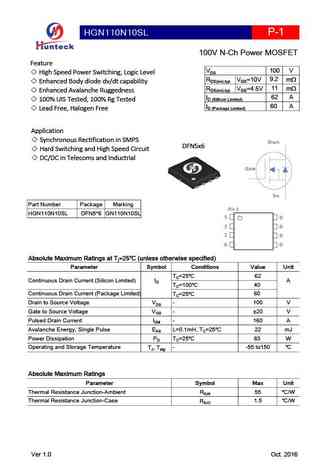
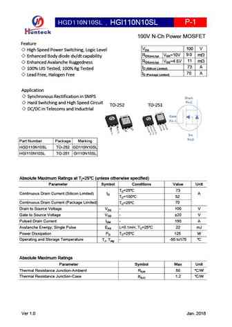
HGN110N10SL P-1 100V N-Ch Power MOSFET Feature 100 V VDS High Speed Power Switching, Logic Level 9.2 RDS(on),typ VGS=10V m Enhanced Body diode dv/dt capability 11 RDS(on),typ VGS=4.5V m Enhanced Avalanche Ruggedness 62 A ID (Sillicon Limited) 100% UIS Tested, 100% Rg Tested 60 A ID (Package Limited) Lead Free, Halogen Free Application Synchronous... See More ⇒
0.12. Size:830K cn hunteck
hgb110n10sl hgp110n10sl.pdf
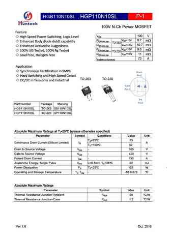
HGB110N10SL , HGP110N10SL P-1 100V N-Ch Power MOSFET Feature 100 V VDS High Speed Power Switching, Logic Level 8.7 RDS(on),typ TO-263 VGS=10V m Enhanced Body diode dv/dt capability VGS=4.5V 10.7 RDS(on),typ m Enhanced Avalanche Ruggedness 9.0 RDS(on),typ TO-220 VGS=10V m 100% UIS Tested, 100% Rg Tested VGS=4.5V 11 RDS(on),typ m Lead Free, Halog... See More ⇒
0.13. Size:793K cn hunteck
hga110n10sl.pdf
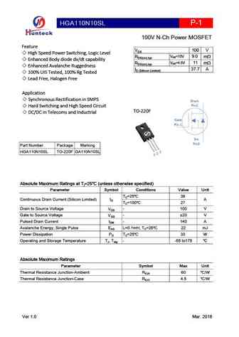
HGA110N10SL P-1 100V N-Ch Power MOSFET Feature 100 V VDS High Speed Power Switching, Logic Level VGS=10V 9.0 RDS(on),typ m Enhanced Body diode dv/dt capability VGS=4.5V 11 RDS(on),typ m Enhanced Avalanche Ruggedness 37.7 A ID (Sillicon Limited) 100% UIS Tested, 100% Rg Tested Lead Free, Halogen Free Application Synchronous Rectification in SMPS ... See More ⇒
0.15. Size:1402K cn apm
apg110n10nf.pdf
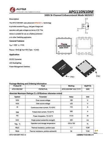
APG110N10NF 100V N-Channel Enhancement Mode MOSFET Description The APG110N10NF uses advanced APM-SGT technology to provide excellent R , low gate charge and DS(ON) operation with gate voltages as low as 4.5V. This device is suitable for use as a Battery protection or in other Switching application. General Features V = 100V I =110A DS D R ... See More ⇒
Detailed specifications: G11
, G16
, G17
, 03N06
, 05N06
, 100N03
, 100P03
, 10N03
, IRF9540
, 11N10C
, 120N03
, 1402TR
, 1404TR
, 140N10
, ECYA
, G1002
, G1002L
.
History: GD1
Keywords - 110N10 MOSFET specs
110N10 cross reference
110N10 equivalent finder
110N10 pdf lookup
110N10 substitution
110N10 replacement
Learn how to find the right MOSFET substitute. A guide to cross-reference, check specs and replace MOSFETs in your circuits.