120N03 Datasheet. Specs and Replacement
Type Designator: 120N03 📄📄
Type of Transistor: MOSFET
Type of Control Channel: N-Channel
Absolute Maximum Ratings
Pd ⓘ - Maximum Power Dissipation: 120 W
|Vds|ⓘ - Maximum Drain-Source Voltage: 30 V
|Vgs|ⓘ - Maximum Gate-Source Voltage: 20 V
|Id| ⓘ - Maximum Drain Current: 120 A
Tj ⓘ - Maximum Junction Temperature: 175 °C
Electrical Characteristics
Cossⓘ - Output Capacitance: 1350 pF
RDSonⓘ - Maximum Drain-Source On-State Resistance: 0.004 Ohm
Package: TO220
📄📄 Copy
- MOSFET ⓘ Cross-Reference Search
120N03 datasheet
..1. Size:1726K goford
120n03.pdf 
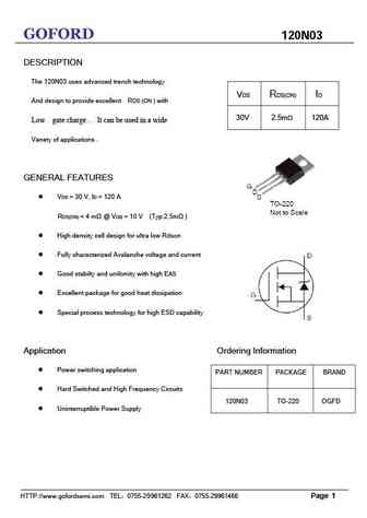
GOFORD 120N03 DESCRIPTION The 120N03 uses advanced trench technology VDS RDS(ON) ID And design to provide excellent RDS (ON ) with 30V 2.5m 120A Low gate charge . It can be used in a wide Vanety of applications . GENERAL FEATURES VDS = 30 V, ID = 120 A RDS(ON) ... See More ⇒
0.1. Size:57K rohm
rss120n03fu6tb rss120n03tb.pdf
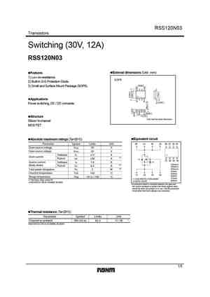
RSS120N03 Transistors Switching (30V, 12A) RSS120N03 External dimensions (Unit mm) Features 1) Low on-resistance. SOP8 2) Built-in G-S Protection Diode. 5.0 0.2 3) Small and Surface Mount Package (SOP8). Applications 0.2 0.1 Power switching, DC / DC converter. 0.4 0.1 1.27 0.1 Structure Each lead has same dimensions Silicon N-channel MOS FET Equivale... See More ⇒
0.2. Size:168K vishay
sqm120n03-1m5l.pdf
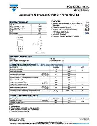
SQM120N03-1m5L Vishay Siliconix Automotive N-Channel 30 V (D-S) 175 C MOSFET FEATURES PRODUCT SUMMARY Halogen-free According to IEC 61249-2-21 VDS (V) 30 Definition RDS(on) ( ) at VGS = 10 V 0.0015 TrenchFET Power MOSFET RDS(on) ( ) at VGS = 4.5 V 0.0020 Package with Low Thermal Resistance ID (A) 120 100 % Rg and UIS Tested Configuration Single AEC-Q10... See More ⇒
0.3. Size:520K infineon
bsc120n03lsg.pdf
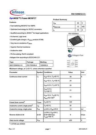
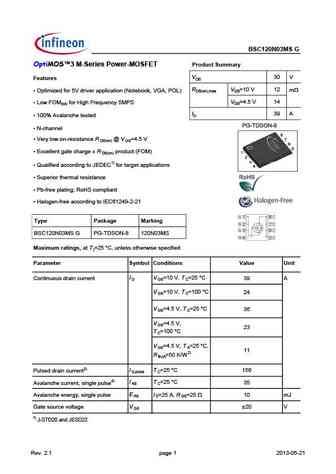
BSC120N03LS G OptiMOS 3 Power-MOSFET Product Summary Features VDS 30 V Fast switching MOSFET for SMPS RDS(on),max 12 mW Optimized technology for DC/DC converters ID 39 A Qualified according to JEDEC1) for target applications PG-TDSON-8 N-channel; Logic level Excellent gate charge x R product (FOM) DS(on) Very low on-resistance R DS(on) Superi... See More ⇒
0.4. Size:524K infineon
bsc120n03msg.pdf
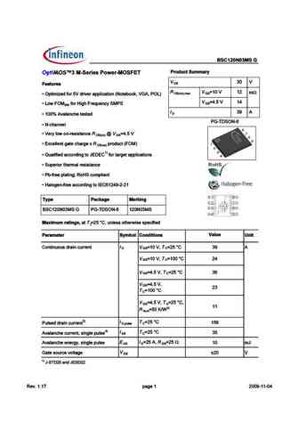
BSC120N03MS G OptiMOS 3 M-Series Power-MOSFET Product Summary VDS 30 V Features RDS(on),max VGS=10 V 12 mW Optimized for 5V driver application (Notebook, VGA, POL) VGS=4.5 V 14 Low FOMSW for High Frequency SMPS ID 39 A 100% Avalanche tested PG-TDSON-8 N-channel Very low on-resistance R @ V =4.5 V DS(on) GS Excellent gate charge x R product (FOM) ... See More ⇒
0.5. Size:485K infineon
bsc120n03ms.pdf

BSC120N03MS G OptiMOS 3 M-Series Power-MOSFET Product Summary VDS 30 V Features RDS(on),max VGS=10 V 12 mW Optimized for 5V driver application (Notebook, VGA, POL) VGS=4.5 V 14 Low FOMSW for High Frequency SMPS ID 39 A 100% Avalanche tested PG-TDSON-8 N-channel Very low on-resistance R @ V =4.5 V DS(on) GS Excellent gate charge x R product (FOM) ... See More ⇒
0.6. Size:686K infineon
bsc120n03ls .pdf
& " & E $;B1= !#& ' $=;0@/? &@99-=D Features D Q 2CD CG D49 ?8 ') - . 7@B -'*- 1 m D n) m x Q ) AD > J65 D649?@=@8I 7@B 4@?F6BD6BC D 1) Q + E2= 7 65 244@B5 ?8 D@ $ 7@B D2B86D 2AA= 42D @?C G D ON Q ( 492??6= &@8 4 =6F6= Q H46==6?D 82D6 492B86 H AB@5E4D ) ' D n) Q /6BI =@G @? B6C CD2?46 D n) Q -EA6B @B D96B>2= B6C CD2?46 Q F2=2?496 B2D65 Q *3 7B66 A=2D ?8 , @... See More ⇒
0.7. Size:481K infineon
bsc120n03ls.pdf

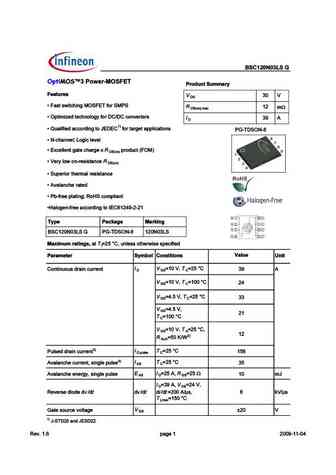
BSC120N03LS G OptiMOS 3 Power-MOSFET Product Summary Features VDS 30 V Fast switching MOSFET for SMPS RDS(on),max 12 mW Optimized technology for DC/DC converters ID 39 A Qualified according to JEDEC1) for target applications PG-TDSON-8 N-channel; Logic level Excellent gate charge x R product (FOM) DS(on) Very low on-resistance R DS(on) Superi... See More ⇒
0.8. Size:678K infineon
bsc120n03msg7.pdf
% ! % # %?88, S 07DK >AI A@ D7E;EF3@57 0 D n) G S J57>>7@F 93F7 5 3D97 J BDA6G5F !* ( D n) 1) S , G3>;8;76 355AD6;@9 FA % 8AD F3D97F 3BB>;53F;A@E S .GB7D;AD F 7... See More ⇒
0.9. Size:277K infineon
ipb120n03s4l-03.pdf
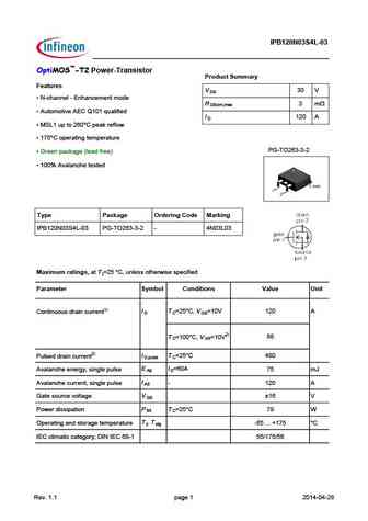
IPB120N03S4L-03 OptiMOS -T2 Power-Transistor Product Summary Features V 30 V DS N-channel - Enhancement mode R 3 mW DS(on),max Automotive AEC Q101 qualified I 120 A D MSL1 up to 260 C peak reflow 175 C operating temperature PG-TO263-3-2 Green package (lead free) 100% Avalanche tested Type Package Ordering Code Marking IPB120N03S4L-03 PG-TO263-3-2 -... See More ⇒
0.10. Size:190K utc
ut120n03.pdf
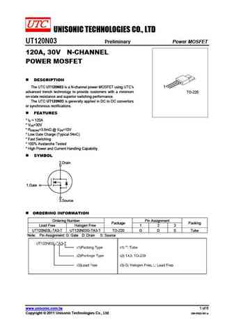
UNISONIC TECHNOLOGIES CO., LTD UT120N03 Preliminary Power MOSFET 120A, 30V N-CHANNEL POWER MOSFET DESCRIPTION The UTC UT120N03 is a N-channel power MOSFET using UTC s 1 advanced trench technology to provide customers with a minimum TO-220 on-state resistance and superior switching performance. The UTC UT120N03 is generally applied in DC to DC convertors or synchronous recti... See More ⇒
0.11. Size:1299K blue-rocket-elect
brcs120n03ya.pdf
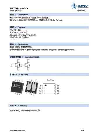
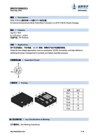
BRCS120N03YA Rev.A May.-2022 DATA SHEET / Descriptions PDFN3 3-8L N MOS Double N-CHANNEL MOSFET in a PDFN3 3-8L Plastic Package. / Features VDS (V) = 30V ID =24A (VGS = 20V) RDS(ON)@10V 13mR(Typ.11mR) HF Product. / Applications Intended for use in g... See More ⇒
0.13. Size:769K blue-rocket-elect
brcs120n03zb.pdf
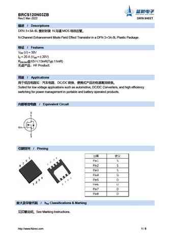
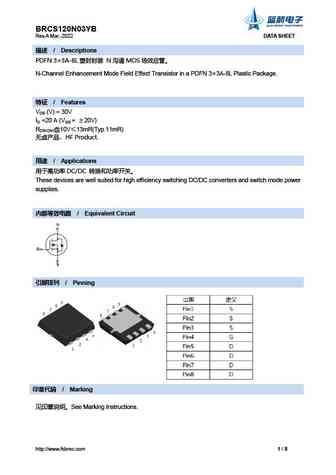
BRCS120N03ZB Rev.C Mar.-2022 DATA SHEET / Descriptions DFN 3 3A-8L N MOS N-Channel Enhancement Mode Field Effect Transistor in a DFN 3 3A-8L Plastic Package. / Features VDS (V) = 30V ID = 20 A (VGS = 20V) RDS(ON)@10V 13mR(Typ.11mR) HF Product. / Applications ... See More ⇒
0.14. Size:1747K blue-rocket-elect
brcs120n03dp.pdf
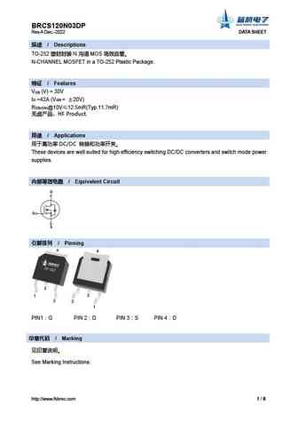
BRCS120N03DP Rev.A Dec.-2022 DATA SHEET / Descriptions TO-252 N MOS N-CHANNEL MOSFET in a TO-252 Plastic Package. / Features V (V) = 30V DS I =42A (V = 20V) D GS R DS(ON)@10V 12.5mR(Typ.11.7mR) HF Product. / Applications DC/DC These devices are well su... See More ⇒
0.16. Size:1114K feihonltd
fhu120n03c fhd120n03c.pdf
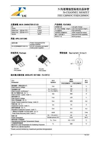
N N-CHANNEL MOSFET FHU120N03C/FHD120N03C MAIN CHARACTERISTICS FEATURES ID 120 A Low gate charge VDSS 30 V Crss ( 120pF) Low Crss (typical 120pF ) Rdson-typ @Vgs=10V 3.0m Fast switching Rdson-typ @Vgs=4.5V 3.7m 100% 100% avalanche teste... See More ⇒
0.17. Size:4803K maple semi
sld120n03tb.pdf
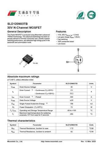
SLD120N03TB 30V N-Channel MOSFET General Description Features This Power MOSFET is produced using Msemitek s advanced 111A, 30V, RDS(on),Typ = 2.5m TRENCH technology. This advanced technology has been es- Low gate charge (Qg,typ = 65nC) pecially tailored to minimize conduction loss, provide superior Fast switching switching performance, and withstand high energy pulse in... See More ⇒
0.18. Size:1172K slkor
sl120n03r.pdf
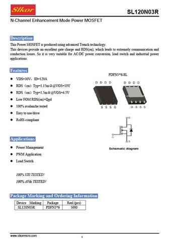
SL120N03R N-Channel Enhancement Mode Power MOSFET Description This Power MOSFET is produced using advanced Trench technology. This devices provide an excellent gate charge and RDS(on), which leads to extremely communication and conduction losses. So it is very suitable for AC/DC power conversion, load switch and industrial power applications. Features PDFN5*6-8L VDS=30V I... See More ⇒
0.21. Size:879K jiejie micro
jmtk120n03a.pdf
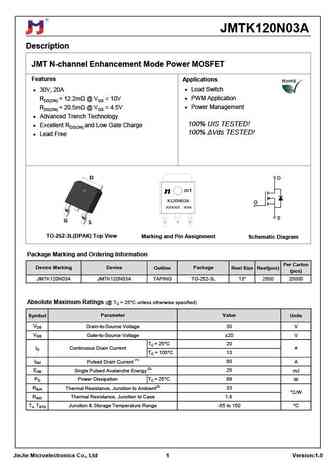
JMTK120N03A Description JMT N-channel Enhancement Mode Power MOSFET Features Applications 30V, 20A Load Switch RDS(ON) ... See More ⇒
0.22. Size:526K jiejie micro
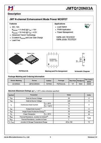
jmtq120n03d.pdf

JMTQ120N03D Description JMT N-channel Enhancement Mode Power MOSFET Features Applications Load Switch 30V, 15A PWM Application RDS(ON) ... See More ⇒
0.23. Size:424K jiejie micro
jmtv120n03a.pdf
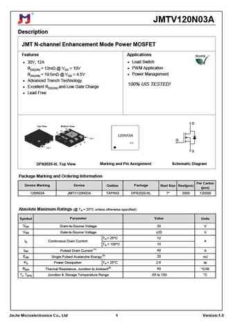
JMTV120N03A Description JMT N-channel Enhancement Mode Power MOSFET Features Applications 30V, 12A Load Switch RDS(ON) ... See More ⇒
0.24. Size:479K jiejie micro
jmtq120n03a.pdf
JMTQ120N03A Description JMT N-channel Enhancement Mode Power MOSFET Features Applications 30V, 18A Load Switch RDS(ON) ... See More ⇒
0.25. Size:895K cn hunteck
hts120n03.pdf
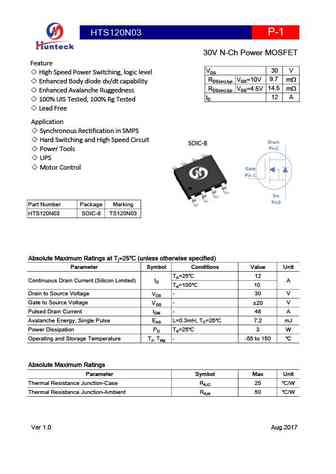
HTS120N03 P-1 30V N-Ch Power MOSFET Feature 30 V VDS High Speed Power Switching, logic level 9.7 RDS(on),typ VGS=10V m Enhanced Body diode dv/dt capability 14.5 RDS(on),typ VGS=4.5V m Enhanced Avalanche Ruggedness 12 A ID 100% UIS Tested, 100% Rg Tested Lead Free Application Synchronous Rectification in SMPS Hard Switching and High Speed Circu... See More ⇒
0.26. Size:902K cn hunteck
htm120n03.pdf
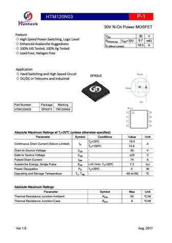
HTM120N03 P-1 30V N-Ch Power MOSFET Feature 30 V VDS High Speed Power Switching, Logic Level 9.7 RDS(on),typ VGS=10V m Enhanced Avalanche Ruggedness 18.5 A ID (Sillicon Limited) 100% UIS Tested, 100% Rg Tested Lead Free, Halogen Free Application Hard Switching and High Speed Circuit Drain DFN3x3 DC/DC in Telecoms and Inductrial Gate Src Part Number ... See More ⇒
0.27. Size:1047K cn hunteck
htm120n03p.pdf
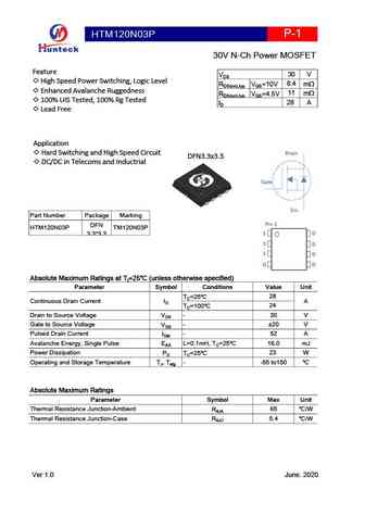
HTM120N03P P-1 30V N-Ch Power MOSFET Feature 30 V VDS High Speed Power Switching, Logic Level 8.4 RDS(on),typ VGS=10V mW Enhanced Avalanche Ruggedness 11 RDS(on),typ VGS=4.5V mW 100% UIS Tested, 100% Rg Tested 28 A ID Lead Free Application Hard Switching and High Speed Circuit Drain DFN3.3x3.3 DC/DC in Telecoms and Inductrial Gate Src Part Number Pa... See More ⇒
0.28. Size:1414K cn vbsemi
vbzqa120n03.pdf
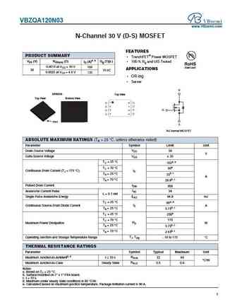
VBZQA120N03 www.VBsemi.com N-Channel 30 V (D-S) MOSFET FEATURES PRODUCT SUMMARY TrenchFET Power MOSFET VDS (V) RDS(on) ( ) ID (A)a, e Qg (Typ.) 100 % Rg and UIS Tested 0.0018 at VGS = 10 V 160 APPLICATIONS 30 18 nC 0.0025 at VGS = 4.5 V 130 OR-ing Server D DFN5X6 Top View Top View Bottom View 1 8 2 7 3 6 G 4 5 PIN1 S N-Channel MOSFET ABSOLU... See More ⇒
0.29. Size:449K cn wuxi unigroup
ttd120n03at ttp120n03at.pdf
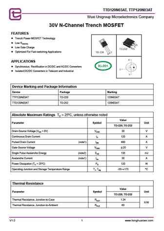
TTD120N03AT, TTP120N03AT Wuxi Unigroup Microelectronics Company 30V N-Channel Trench MOSFET FEATURES Trench Power MOSFET Technology Low RDS(ON) Low Gate Charge Optimized For Fast-switching Applications APPLICATIONS Synchronous Rectification in DC/DC and AC/DC Converters Isolated DC/DC Converters in Telecom and Industrial Device Marking and Package ... See More ⇒
0.30. Size:594K cn hmsemi
hm120n03.pdf
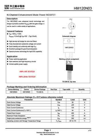
HM120N03 N-Channel Enhancement Mode Power MOSFET Description The HM120N03 uses advanced trench technology and design to provide excellent RDS(ON) with low gate charge. It can be used in a wide variety of applications. General Features VDS =30V,ID =120A RDS(ON) ... See More ⇒
0.31. Size:573K cn hmsemi
hms120n03d.pdf
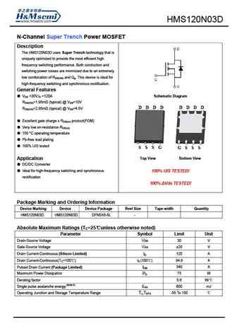
HMS120N03D N-Channel Super Trench Power MOSFET Description The HMS120N03D uses Super Trench technology that is uniquely optimized to provide the most efficient high frequency switching performance. Both conduction and switching power losses are minimized due to an extremely low combination of RDS(ON) and Qg. This device is ideal for high-frequency switching and synchronous rectif... See More ⇒
0.32. Size:559K cn hmsemi
hm120n03k.pdf
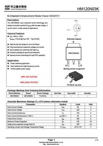
N-Channel Enhancement Mode Power MOSFET Description The uses advanced trench technology and design to provide excellent RDS(ON) with low gate charge. It can be used in a wide variety of applications. General Features VDS =30V,ID =120A RDS(ON) ... See More ⇒
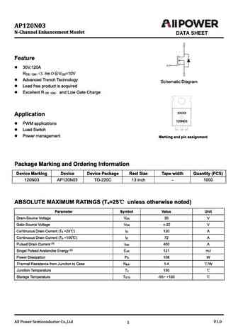
0.33. Size:1444K cn apm
ap120n03nf.pdf
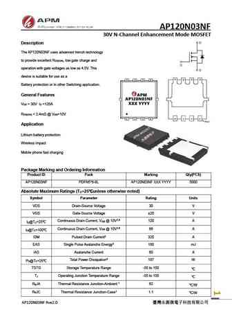
AP120N03NF 30V N-Channel Enhancement Mode MOSFET Description The AP120N03NF uses advanced trench technology to provide excellent R , low gate charge and DS(ON) operation with gate voltages as low as 4.5V. This device is suitable for use as a Battery protection or in other Switching application. General Features V = 30V I =120A DS D R ... See More ⇒
0.34. Size:1481K cn apm
ap120n03d.pdf
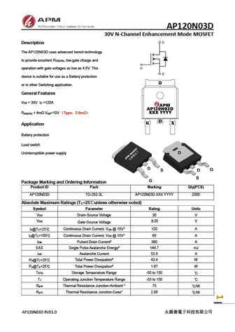
AP120N03D 30V N-Channel Enhancement Mode MOSFET Description The AP120N03D uses advanced trench technology to provide excellent R , low gate charge and DS(ON) operation with gate voltages as low as 4.5V. This device is suitable for use as a Battery protection or in other Switching application. General Features V = 30V I =120A DS D R ... See More ⇒
Detailed specifications: G17, 03N06, 05N06, 100N03, 100P03, 10N03, 110N10, 11N10C, STP75NF75, 1402TR, 1404TR, 140N10, ECYA, G1002, G1002L, G1003A, G1006
Keywords - 120N03 MOSFET specs
120N03 cross reference
120N03 equivalent finder
120N03 pdf lookup
120N03 substitution
120N03 replacement
Can't find your MOSFET?
Learn how to find a substitute transistor by analyzing voltage, current and package compatibility