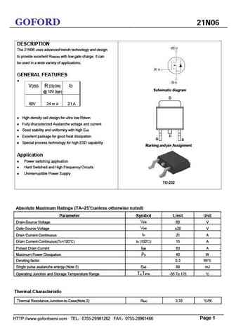
21N06 Specs and Replacement
Type Designator: 21N06
Type of Transistor: MOSFET
Type of Control Channel: N-Channel
Absolute Maximum Ratings
Pd ⓘ
- Maximum Power Dissipation: 45 W
|Vds|ⓘ - Maximum Drain-Source Voltage: 60 V
|Vgs|ⓘ - Maximum Gate-Source Voltage: 20 V
|Id| ⓘ - Maximum Drain Current: 21 A
Tj ⓘ - Maximum Junction Temperature: 175 °C
Electrical Characteristics
tr ⓘ - Rise Time: 2.9 nS
Cossⓘ -
Output Capacitance: 102 pF
RDSonⓘ - Maximum Drain-Source On-State Resistance: 0.03 Ohm
Package: TO252
- MOSFET ⓘ Cross-Reference Search
21N06 datasheet
0.1. Size:113K philips
phd21n06lt.pdf 

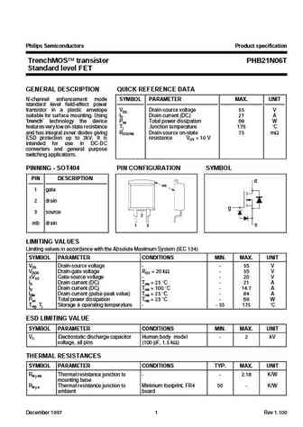
Philips Semiconductors Product specification N-channel TrenchMOS transistor PHP21N06LT, PHB21N06LT Logic level FET PHD21N06LT FEATURES SYMBOL QUICK REFERENCE DATA Trench technology d VDSS = 55 V Low on-state resistance Fast switching ID = 19 A Logic level compatible RDS(ON) 75 m (VGS = 5 V) g RDS(ON) 70 m (VGS = 10 V) s GENERAL DESCRIPTION ... See More ⇒
0.2. Size:56K philips
phb21n06t 1.pdf
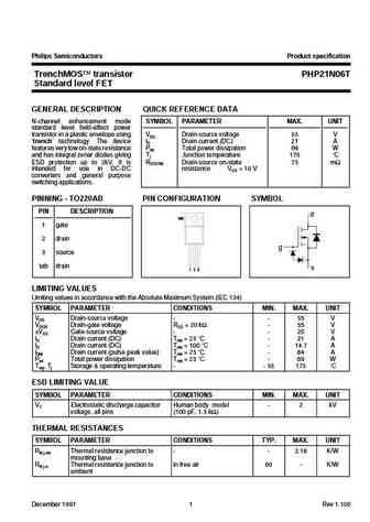
Philips Semiconductors Product specification TrenchMOS transistor PHB21N06T Standard level FET GENERAL DESCRIPTION QUICK REFERENCE DATA N-channel enhancement mode SYMBOL PARAMETER MAX. UNIT standard level field-effect power transistor in a plastic envelope VDS Drain-source voltage 55 V suitable for surface mounting. Using ID Drain current (DC) 21 A trench technology the devic... See More ⇒
0.3. Size:52K philips
php21n06t.pdf
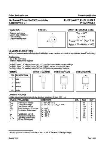
Philips Semiconductors Product specification TrenchMOS transistor PHP21N06T Standard level FET GENERAL DESCRIPTION QUICK REFERENCE DATA N-channel enhancement mode SYMBOL PARAMETER MAX. UNIT standard level field-effect power transistor in a plastic envelope using VDS Drain-source voltage 55 V trench technology. The device ID Drain current (DC) 21 A features very low on-state r... See More ⇒
0.4. Size:114K philips
phb21n06lt phd21n06lt php21n06lt.pdf
Philips Semiconductors Product specification N-channel TrenchMOS transistor PHP21N06LT, PHB21N06LT Logic level FET PHD21N06LT FEATURES SYMBOL QUICK REFERENCE DATA Trench technology d VDSS = 55 V Low on-state resistance Fast switching ID = 19 A Logic level compatible RDS(ON) 75 m (VGS = 5 V) g RDS(ON) 70 m (VGS = 10 V) s GENERAL DESCRIPTION ... See More ⇒
0.5. Size:197K st
stp21n06.pdf
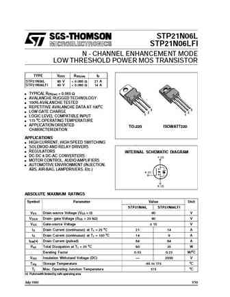
STP21N06L STP21N06LFI N - CHANNEL ENHANCEMENT MODE LOW THRESHOLD POWER MOS TRANSISTOR TYPE V R I DSS DS(on) D STP21N06L 60 V ... See More ⇒
0.6. Size:383K st
stp21n06l.pdf
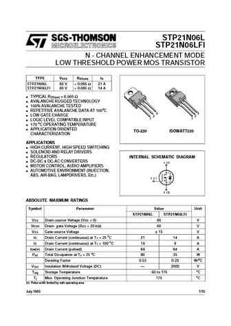
STP21N06L STP21N06LFI N - CHANNEL ENHANCEMENT MODE LOW THRESHOLD POWER MOS TRANSISTOR TYPE VDSS RDS(on) ID STP21N06L 60 V ... See More ⇒
0.7. Size:229K nxp
php21n06lt phb21n06lt phd21n06lt.pdf

Important notice Dear Customer, On 7 February 2017 the former NXP Standard Product business became a new company with the tradename Nexperia. Nexperia is an industry leading supplier of Discrete, Logic and PowerMOS semiconductors with its focus on the automotive, industrial, computing, consumer and wearable application markets In data sheets and application notes which still contain... See More ⇒
0.8. Size:366K rohm
rsd221n06.pdf
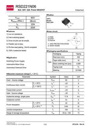
RSD221N06 Nch 60V 22A Power MOSFET Datasheet lOutline VDSS 60V CPT3 (SC-63) RDS(on) (Max.) 26mW (3) ID 22A (2) (1) PD 20W lFeatures lInner circuit (3) 1) Low on-resistance. (1) Gate *1 2) Fast switching speed. (2) Drain (3) Source (1) 3) Drive circuits can be simple. *2 *1 ESD PROTECTION DIODE 4) Parallel use is easy. *2 BODY DIODE 5) Pb-free... See More ⇒
0.9. Size:891K rohm
rsd221n06fra.pdf
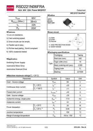
RSD221N06FRA Nch 60V 22A Power MOSFET Datasheet AEC-Q101 Qualified lOutline VDSS 60V CPT3 (SC-63) RDS(on) (Max.) 26mW (3) ID 22A (2) (1) PD 20W lFeatures lInner circuit (3) 1) Low on-resistance. (1) Gate *1 2) Fast switching speed. (2) Drain (3) Source (1) 3) Drive circuits can be simple. *2 *1 ESD PROTECTION DIODE 4) Parallel use is easy. *2 ... See More ⇒
0.10. Size:999K infineon
ipp024n06n3g ipb021n06n3g ipi024n06n3g.pdf
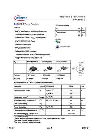
pe IPB021N06N3 G IPI024N06N3 G IPP024N06N3 G 3 Power-Transistor Product Summary Features V D Q #4513I CG9D389>7 1>4 CI>3 B53 R 1 m , ?> =1H ,& Q ( @D9=9J54 D538>?F5BD5BC I 1 D Q H35... See More ⇒
0.11. Size:483K infineon
ipb021n06n3g ipi024n06n3g ipp024n06n3g.pdf
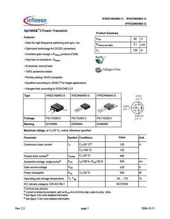
Type IPB021N06N3 G IPI024N06N3 G IPP024N06N3 G OptiMOS 3 Power-Transistor Product Summary Features V 60 V DS Ideal for high frequency switching and sync. rec. R 2.1 m DS(on),max (SMD) Optimized technology for DC/DC converters I 120 A D Excellent gate charge x R product (FOM) DS(on) Very low on-resistance RDS(on) N-channel, normal level 100% avalanch... See More ⇒
0.12. Size:772K cn hunteck
hgn021n06sl.pdf
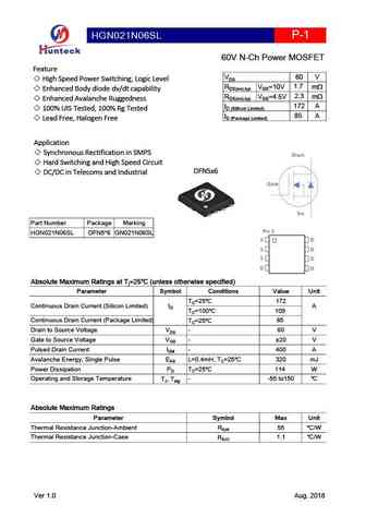
HGN021N06SL P-1 60V N-Ch Power MOSFET Feature 60 V VDS High Speed Power Switching, Logic Level 1.7 RDS(on),typ VGS=10V m Enhanced Body diode dv/dt capability 2.3 RDS(on),typ VGS=4.5V m Enhanced Avalanche Ruggedness 172 A ID (Sillicon Limited) 100% UIS Tested, 100% Rg Tested 85 A ID (Package Limited) Lead Free, Halogen Free Application Synchronous... See More ⇒
0.13. Size:228K inchange semiconductor
ipb021n06n3g.pdf
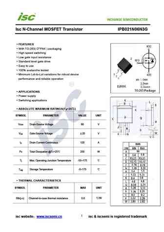
Isc N-Channel MOSFET Transistor IPB021N06N3G FEATURES With TO-263( D PAK ) packaging High speed switching Low gate input resistance Standard level gate drive Easy to use 100% avalanche tested Minimum Lot-to-Lot variations for robust device performance and reliable operation APPLICATIONS Power supply Switching applications ABSOLUTE MAXIMUM RATINGS(T =25 ) ... See More ⇒
Detailed specifications: G1815
, G1816
, G1825
, 15P03
, 16N10
, 18N10
, 2002A
, 20P10
, AO3407
, 22N10
, 2301H
, 2301L
, 25P06
, 25P10
, 25P10G
, 28N10
, 28P55
.
History: CPH5901
Keywords - 21N06 MOSFET specs
21N06 cross reference
21N06 equivalent finder
21N06 pdf lookup
21N06 substitution
21N06 replacement
Step-by-step guide to finding a MOSFET replacement. Cross-reference parts and ensure compatibility for your repair or project.