18N20 Datasheet. Specs and Replacement
Type Designator: 18N20 📄📄
Type of Transistor: MOSFET
Type of Control Channel: N-Channel
Absolute Maximum Ratings
Pd ⓘ - Maximum Power Dissipation: 110 W
|Vds|ⓘ - Maximum Drain-Source Voltage: 200 V
|Vgs|ⓘ - Maximum Gate-Source Voltage: 30 V
|Id| ⓘ - Maximum Drain Current: 18 A
Tj ⓘ - Maximum Junction Temperature: 150 °C
Electrical Characteristics
tr ⓘ - Rise Time: 21.1 nS
Cossⓘ - Output Capacitance: 81.2 pF
📄📄 Copy
18N20 substitution
- MOSFET ⓘ Cross-Reference Search
18N20 datasheet
18n20.pdf
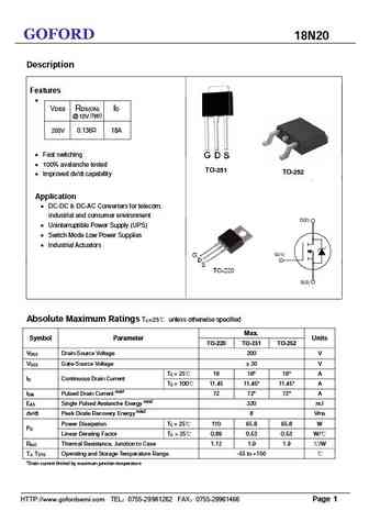
GOFORD 18N20 Description Features VDSS RDS(ON) ID @ 10V (typ) 0.136 18A 200V Fast switching 100% avalanche tested TO-251 TO-252 Improved dv/dt capability Application DC-DC & DC-AC Converters for telecom, industrial and consumer environment Uninterruptible Power Supply (UPS) Switch Mode Low Power Supplies Industrial Actuators... See More ⇒
18n20.pdf
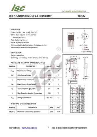
isc N-Channel MOSFET Transistor 18N20 FEATURES Drain Current I = 18A@ T =25 D C Static drain-source on-resistance RDS(on) 0.092 Fast Switching Speed 100% avalanche tested Minimum Lot-to-Lot variations for robust device performance and reliable operation DESCRITION Switch regulators Switching converters, motor drivers, relay drivers ABSOLUTE MAXIMUM RAT... See More ⇒
php18n20e 1.pdf
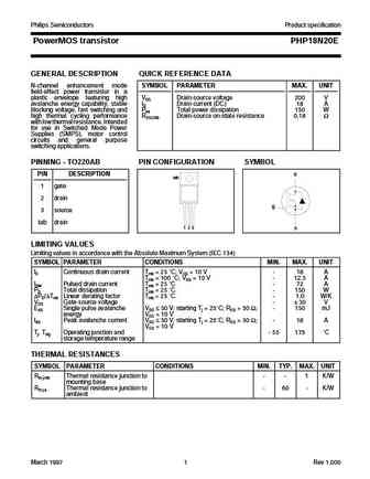
Philips Semiconductors Product specification PowerMOS transistor PHP18N20E GENERAL DESCRIPTION QUICK REFERENCE DATA N-channel enhancement mode SYMBOL PARAMETER MAX. UNIT field-effect power transistor in a plastic envelope featuring high VDS Drain-source voltage 200 V avalanche energy capability, stable ID Drain current (DC) 18 A blocking voltage, fast switching and Ptot Total power dis... See More ⇒
stb18n20.pdf
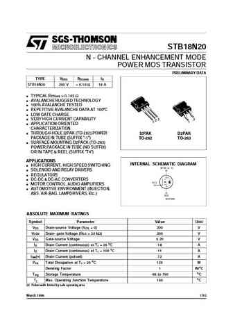
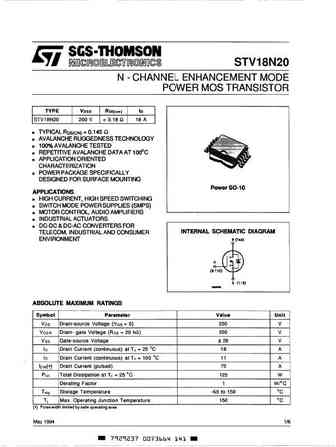
STB18N20 N - CHANNEL ENHANCEMENT MODE POWER MOS TRANSISTOR PRELIMINARY DATA TYPE V R I DSS DS(on) D STB18N20 200 V ... See More ⇒
fdpf18n20ft g.pdf
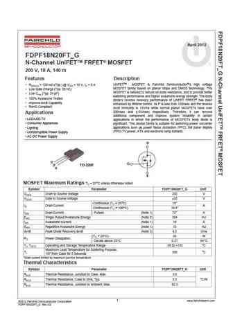
April 2013 FDPF18N20FT_G N-Channel UniFETTM FRFET MOSFET 200 V, 18 A, 140 m Features Description UniFETTM MOSFET is Fairchild Semiconductor s high voltage RDS(on) = 129 m (Typ.) @ VGS = 10 V, ID = 9 A MOSFET family based on planar stripe and DMOS technology. This Low Gate Charge (Typ. 20 nC) MOSFET is tailored to reduce on-state resistance, and to provide bette... See More ⇒
fdpf18n20f.pdf
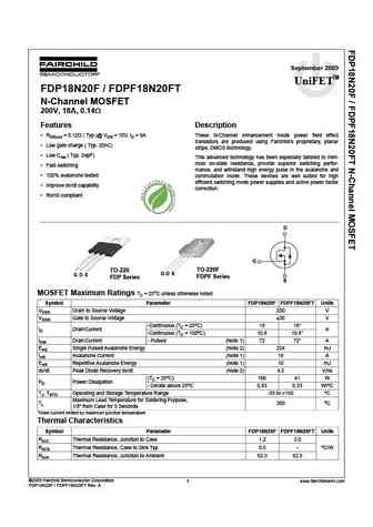
September 2009 UniFETTM FDP18N20F / FDPF18N20FT tm N-Channel MOSFET 200V, 18A, 0.14 Features Description RDS(on) = 0.12 ( Typ.)@ VGS = 10V, ID = 9A These N-Channel enhancement mode power field effect transistors are produced using Fairchild s proprietary, planar Low gate charge ( Typ. 20nC) stripe, DMOS technology. Low Crss ( Typ. 24pF) This advanced technology h... See More ⇒
fdp18n20f fdpf18n20f.pdf

September 2009 UniFETTM FDP18N20F / FDPF18N20FT tm N-Channel MOSFET 200V, 18A, 0.14 Features Description RDS(on) = 0.12 ( Typ.)@ VGS = 10V, ID = 9A These N-Channel enhancement mode power field effect transistors are produced using Fairchild s proprietary, planar Low gate charge ( Typ. 20nC) stripe, DMOS technology. Low Crss ( Typ. 24pF) This advanced technology h... See More ⇒
fqp18n20v2 fqpf18n20v2.pdf
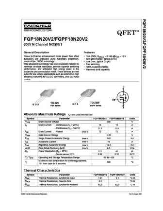
TM QFET FQP18N20V2/FQPF18N20V2 200V N-Channel MOSFET General Description Features These N-Channel enhancement mode power field effect 18A, 200V, RDS(on) = 0.14 @VGS = 10 V transistors are produced using Fairchild s proprietary, Low gate charge ( typical 20 nC) planar stripe, DMOS technology. Low Crss ( typical 25 pF) This advanced technology has been especially tailore... See More ⇒
fqd18n20v2tf fqd18n20v2tm fqd18n20v2 fqu18n20v2.pdf
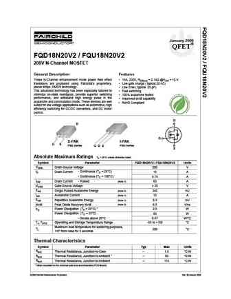
January 2009 QFET FQD18N20V2 / FQU18N20V2 200V N-Channel MOSFET General Description Features These N-Channel enhancement mode power field effect 15A, 200V, RDS(on) = 0.14 @VGS = 10 V transistors are produced using Fairchild s proprietary, Low gate charge ( typical 20 nC) planar stripe, DMOS technology. Low Crss ( typical 25 pF) This advanced technology has been espec... See More ⇒
fdd18n20lz.pdf
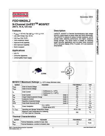
December 2013 FDD18N20LZ N-Channel UniFETTM MOSFET 200 V, 16 A, 125 m Features Description R DS(on) = 125 m (Typ.) @ VGS = 10 V, ID = 8 A UniFETTM MOSFET is Fairchild Semiconductor s high voltage MOSFET family based on planar stripe and DMOS technology. Low Gate Charge (Typ. 30 nC) This MOSFET is tailored to reduce on-state resistance, and to Low CRSS (Typ. 25 pF)... See More ⇒
mcu18n20.pdf
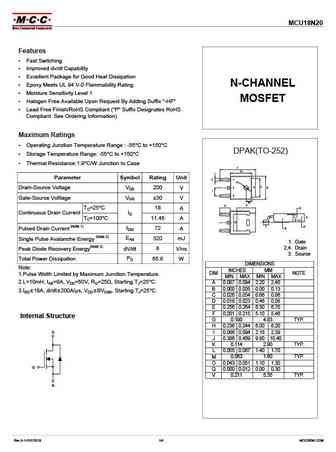
MCU18N20 Features Fast Switching Improved dv/dt Capability Excellent Package for Good Heat Dissipation Epoxy Meets UL 94 V-0 Flammability Rating N-CHANNEL Moisture Sensitivity Level 1 MOSFET Halogen Free Available Upon Request By Adding Suffix "-HF" Lead Free Finish/RoHS Compliant ("P" Suffix Designates RoHS Compliant. See Ordering Information) Maximum Rat... See More ⇒
fdp18n20f fdpf18n20ft.pdf

Is Now Part of To learn more about ON Semiconductor, please visit our website at www.onsemi.com Please note As part of the Fairchild Semiconductor integration, some of the Fairchild orderable part numbers will need to change in order to meet ON Semiconductor s system requirements. Since the ON Semiconductor product management systems do not have the ability to manage part nomenclatur... See More ⇒
fdd18n20lz.pdf
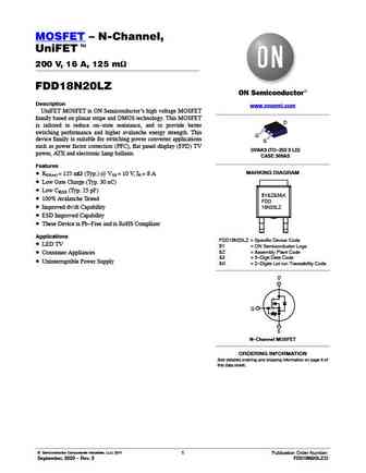
MOSFET N-Channel, UniFETt 200 V, 16 A, 125 mW FDD18N20LZ Description www.onsemi.com UniFET MOSFET is ON Semiconductor s high voltage MOSFET family based on planar stripe and DMOS technology. This MOSFET D is tailored to reduce on-state resistance, and to provide better switching performance and higher avalanche energy strength. This G device family is suitable for switching po... See More ⇒
ap18n20ags-hf.pdf
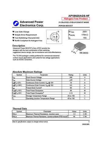
AP18N20AGS-HF Halogen-Free Product Advanced Power N-CHANNEL ENHANCEMENT MODE Electronics Corp. POWER MOSFET D Low Gate Charge BVDSS 200V Simple Drive Requirement RDS(ON) 170m Fast Switching Characteristic ID 18A G RoHS Compliant & Halogen-Free S Description Advanced Power MOSFETs from APEC provide the designer with the best combination of fast switching, G rugge... See More ⇒
ap18n20gh-hf ap18n20gj-hf.pdf
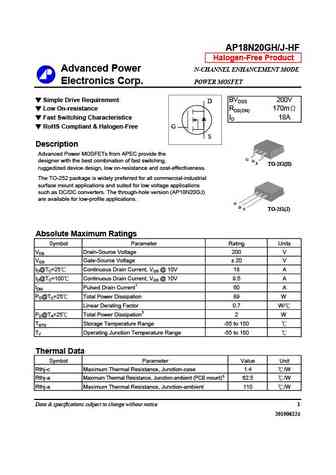
AP18N20GH/J-HF Halogen-Free Product Advanced Power N-CHANNEL ENHANCEMENT MODE Electronics Corp. POWER MOSFET Simple Drive Requirement BVDSS 200V D Low On-resistance RDS(ON) 170m Fast Switching Characteristics ID 18A RoHS Compliant & Halogen-Free G S Description Advanced Power MOSFETs from APEC provide the G designer with the best combination of fast switching, D ... See More ⇒
ap18n20gs.pdf
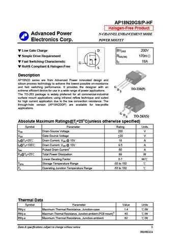
AP18N20GS/P-HF Halogen-Free Product Advanced Power N-CHANNEL ENHANCEMENT MODE Electronics Corp. POWER MOSFET D Low Gate Charge BVDSS 200V Simple Drive Requirement RDS(ON) 170m Fast Switching Characteristic ID 18A G RoHS Compliant & Halogen-Free S Description AP18N20 series are from Advanced Power innovated design and silicon process technology to achieve the lowes... See More ⇒
ap18n20gp-hf ap18n20gs-hf.pdf
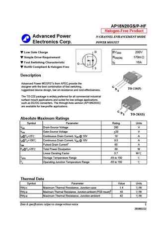
AP18N20GS/P-HF Halogen-Free Product Advanced Power N-CHANNEL ENHANCEMENT MODE Electronics Corp. POWER MOSFET D Low Gate Charge BVDSS 200V Simple Drive Requirement RDS(ON) 170m Fast Switching Characteristic ID 18A G RoHS Compliant & Halogen-Free S Description Advanced Power MOSFETs from APEC provide the designer with the best combination of fast switching, G TO-22... See More ⇒
ap18n20gi.pdf
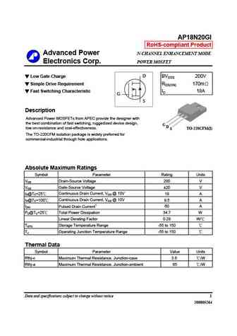
AP18N20GI RoHS-compliant Product Advanced Power N-CHANNEL ENHANCEMENT MODE Electronics Corp. POWER MOSFET D Low Gate Charge BVDSS 200V Simple Drive Requirement RDS(ON) 170m Fast Switching Characteristic ID 18A G S Description Advanced Power MOSFETs from APEC provide the designer with the best combination of fast switching, ruggedized device design, G D low on-resist... See More ⇒
mtn18n20fp.pdf
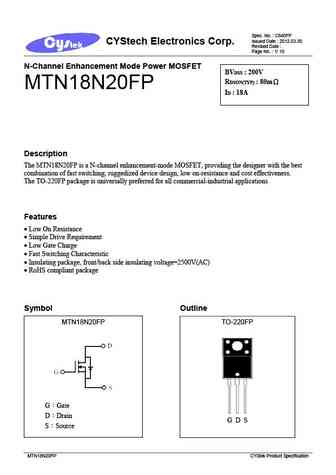
Spec. No. C840FP Issued Date 2012.03.30 CYStech Electronics Corp. Revised Date Page No. 1/ 10 N-Channel Enhancement Mode Power MOSFET BVDSS 200V RDSON(TYP) 80m MTN18N20FP ID 18A Description The MTN18N20FP is a N-channel enhancement-mode MOSFET, providing the designer with the best combination of fast switching, ruggedized device design, low on-resistance a... See More ⇒
18n20a.pdf
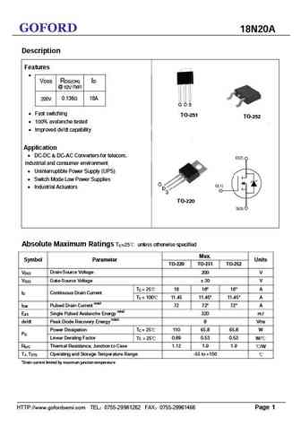
GOFORD 18N20A Description Features VDSS RDS(ON) ID @ 10V (typ) 0.136 18A 200V Fast switching TO-251 TO-252 100% avalanche tested Improved dv/dt capability Application DC-DC & DC-AC Converters for telecom, industrial and consumer environment Uninterruptible Power Supply (UPS) Switch Mode Low Power Supplies Industrial Actuators... See More ⇒
g18n20k.pdf
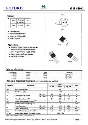
GOFORD G18N20K Features VDSS RDS(ON) ID @ 10V (typ) 0.136 18A 200V Fast switching 100% avalanche tested Improved dv/dt capability RoHS Compliant Application DC-DC & DC-AC Converters for telecom, industrial and consumer environment Uninterruptible Power Supply (UPS) Switch Mode Low Power Supplies Industrial Actuators Orderi... See More ⇒
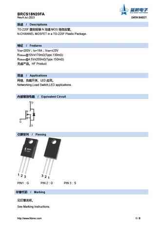
brcs18n20dp.pdf
BRCS18N20DP Rev.B Jul.-2023 DATA SHEET / Descriptions N TO-252 N-Channel MOSFET in a TO-252 Plastic Package. / Features V =200V I =18A V = 20V DS D GS R DS(on)@10V 170m (Type.130m ) R DS(on)@4.5V 200m (Type.150m ) HF Product. / Applications LED Net... See More ⇒
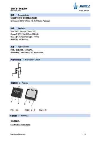
brcs18n20ra.pdf
BRCS18N20RA Rev.B Jun.-2023 DATA SHEET / Descriptions N TO-220 N-Channel MOSFET in a TO-220 Plastic Package. / Features V =200V I =18A V = 20V DS D GS R DS(on)@10V 170m (Type.130m ) R DS(on)@4.5V 200m (Type.150m ) HF Product. / Applications LED Net... See More ⇒
fir18n20g.pdf
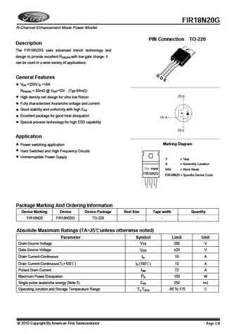
FIR18N20G N-Channel Enhancement Mode Power Mosfet PIN Connection TO-220 Description The FIR18N20G uses advanced trench technology and design to provide excellent RDS(ON) with low gate charge. It can be used in a wide variety of applications. General Features VDS =200V,ID =18A RDS(ON) ... See More ⇒
d18n20.pdf
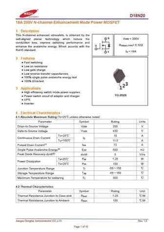
D18N20 18A 200V N-channel Enhancement Mode Power MOSFET 1 Description This N-channel enhanced vdmosfets, is obtained by the 2 D V = 200V self-aligned planar technology which reduce the DSS conduction loss, improve switching performance and R = 0.12 DS(on) (TYP) G enhance the avalanche energy. Which accords with the 1 RoHS standard. I = 18A 3 S D 2 Features Fast switching ... See More ⇒
wfp18n20.pdf
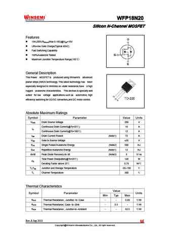
WFP18N20 WFP18N20 WFP18N20 WFP18N20 Silicon N-Channel MOSFET Silicon N-Channel MOSFET Silicon N-Channel MOSFET Silicon N-Channel MOSFET Features 18A,200V,R (Max 0.18 )@V =10V DS(on) GS Ultra-low Gate Charge(Typical 40nC) Fast Switching Capability 100%Avalanche Tested Maximum Junction Temperature Range(150 ) General Description This Power MOSFET is produce... See More ⇒
bl18n20-p bl18n20-a bl18n20-u bl18n20-d.pdf
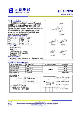
BL18N20 Power MOSFET 1 Description Step-Down Converter BL18N20, the silicon N-channel Enhanced , MOSFETs, is obtained by advanced MOSFET technology which reduce the conduction loss, improve switching performance and enhance the avalanche energy. The transistor is suitable device for SMPS, high speed switching and general purpose applications. KEY CHARACTERISTICS Pa... See More ⇒
ctm18n20.pdf
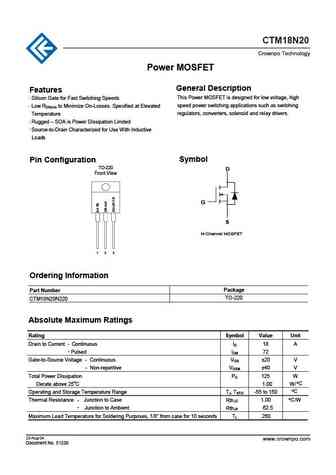
CTM18N20 Crownpo Technology Power MOSFET General Description Features . This Power MOSFET is designed for low voltage, high Silicon Gate for Fast Switching Speeds . speed power switching applications such as switching Low R to Minimize On-Losses. Specified at Elevated DS(on) regulators, converters, solenoid and relay drivers. Temperature . Rugged SOA is Power Dissipation Limi... See More ⇒
hy18n20t.pdf
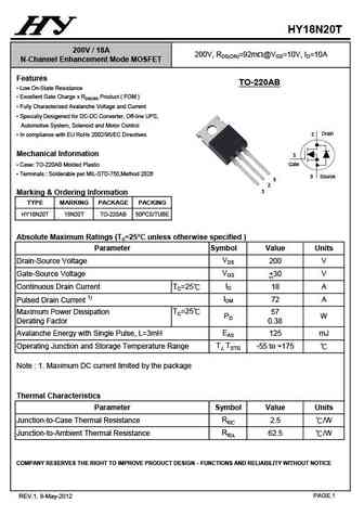
HY18N20T 200V / 18A 200V, RDS(ON)=92mW@VGS=10V, ID=10A N-Channel Enhancement Mode MOSFET Features TO-220AB Low On-State Resistance Excellent Gate Charge x RDS(ON) Product ( FOM ) Fully Characterized Avalanche Voltage and Current Specially Desigened for DC-DC Converter, Off-line UPS, Automotive System, Solenoid and Motor Control Drain 2 In compliance with E... See More ⇒
hy18n20d.pdf
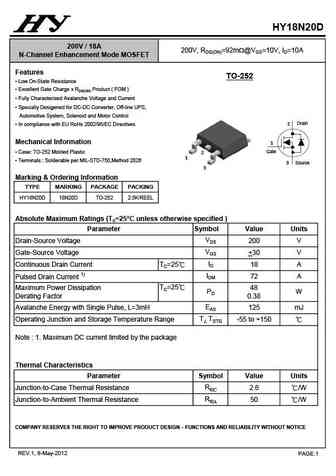
HY18N20D 200V / 18A 200V, RDS(ON)=92mW@VGS=10V, ID=10A N-Channel Enhancement Mode MOSFET Features TO-252 Low On-State Resistance Excellent Gate Charge x RDS(ON) Product ( FOM ) Fully Characterized Avalanche Voltage and Current Specially Desigened for DC-DC Converter, Off-line UPS, Automotive System, Solenoid and Motor Control Drain 2 In compliance with EU R... See More ⇒
ptp18n20a.pdf
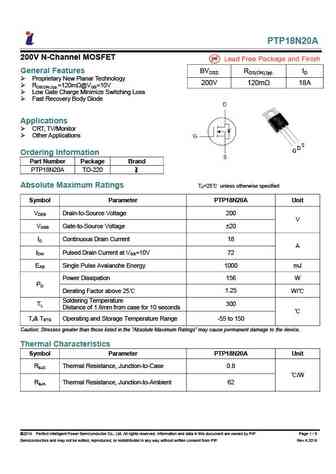
PTP18N20A 200V N-Channel MOSFET General Features BVDSS RDS(ON),typ. ID Proprietary New Planar Technology 200V 120m 18A RDS(ON),typ.=120m @VGS=10V Low Gate Charge Minimize Switching Loss Fast Recovery Body Diode Applications CRT, TV/Monitor Other Applications S G D Ordering Information Part Number Package Brand PTP18N20A TO-220 Absolut... See More ⇒
wvm18n20.pdf

Shaanxi Qunli Electric Co., Ltd Add. No. 1 Qunli Road,Baoji City,Shaanxi,China WVM18N20(IRF240) Power MOSFET(N-channel) Transistor Features 1. It s voltage control component with good input impedance, small starting power dissipation, wide area of safe operation, good temperature stability. 2. Implementation of standards QZJ840611 3. Use for high speed switch, circuit of power s... See More ⇒
sl18n20.pdf
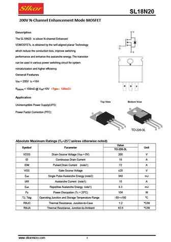
SL18N20 200V N-Channel Enhancement Mode MOSFET Description is silicon N-channel Enhanced The SL18N20 VDMOSFETs, is obtained by the self-aligned planar Technology which reduce the conduction loss, improve switching performance and enhance the avalanche energy. The transistor can be used in various power switching circuit for system miniaturization and higher efficiency. General... See More ⇒
tmd18n20z tmu18n20z.pdf
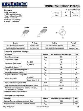
TMD18N20Z(G)/TMU18N20Z(G) N-channel MOSFET Features Low gate charge BVDSS ID RDS(on) MAX 100% avalanche tested 200V 18A ... See More ⇒
tmp18n20z tmpf18n20z.pdf
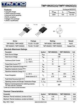
TMP18N20Z(G)/TMPF18N20Z(G) N-channel MOSFET Features Low gate charge BVDSS ID RDS(on)MAX 100% avalanche tested 200V 18A ... See More ⇒
tsd18n20m.pdf
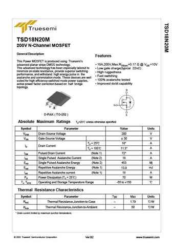
TSD18N20M 200V N-Channel MOSFET General Description Features This Power MOSFET is produced using Truesemi s 18A,200V,Max.RDS(on)=0.17 @ VGS =10V advanced planar stripe DMOS technology. This advanced technology has been especially tailored to Low gate charge(typical 22nC) minimize on-state resistance, provide superior switching High ruggedness performance, an... See More ⇒
tsf18n20m.pdf
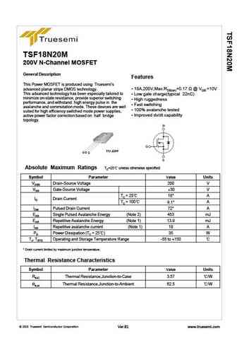
TSF18N20M 200V N-Channel MOSFET General Description Features This Power MOSFET is produced using Truesemi s 18A,200V,Max.RDS(on)=0.17 @ VGS =10V advanced planar stripe DMOS technology. This advanced technology has been especially tailored to Low gate charge(typical 22nC) minimize on-state resistance, provide superior switching High ruggedness performance, ... See More ⇒
wmo18n20t2.pdf
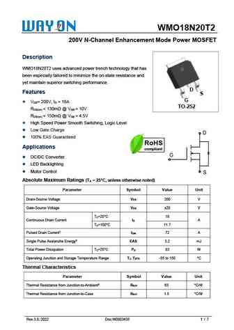
WMO18N20T2 200V N-Channel Enhancement Mode Power MOSFET Description WMO18N20T2 uses advanced power trench technology that has been especially tailored to minimize the on-state resistance and yet maintain superior switching performance. D Features S G V = 200V, I = 18A DS D TO-252 R ... See More ⇒
cs18n20bf cs18n20bp cs18n20bb.pdf
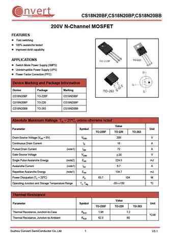
nvert Suzhou Convert Semiconductor Co ., Ltd. CS18N20BF,CS18N20BP,CS18N20BB 200V N-Channel MOSFET FEATURES Fast switching 100% avalanche tested Improved dv/dt capability APPLICATIONS Switch Mode Power Supply (SMPS) Uninterruptible Power Supply (UPS) Power Factor Correction (PFC) Device Marking and Package Information Device Package Marking CS18N20BF TO-220F... See More ⇒
cs18n20bf cs18n20bp.pdf
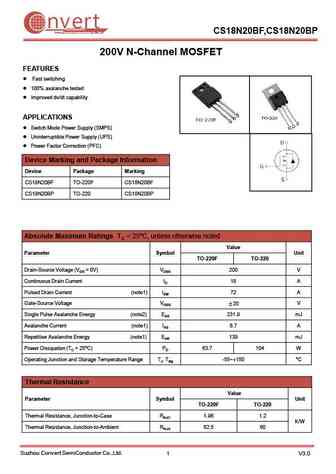
nvert Suzhou Convert Semiconductor Co ., Ltd. CS18N20BF,CS18N20BP 200V N-Channel MOSFET FEATURES Fast switching 100% avalanche tested Improved dv/dt capability APPLICATIONS Switch Mode Power Supply (SMPS) Uninterruptible Power Supply (UPS) Power Factor Correction (PFC) Device Marking and Package Information Device Package Marking CS18N20BF TO-220F CS18N20BF... See More ⇒
hsp18n20.pdf
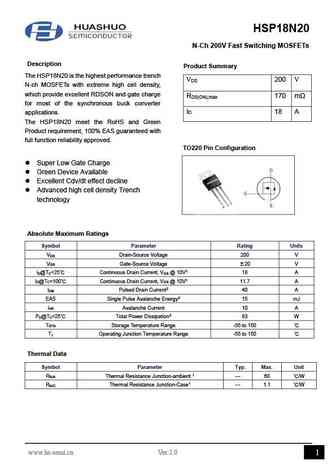
HSP18N20 N-Ch 200V Fast Switching MOSFETs Description Product Summary The HSP18N20 is the highest performance trench V 200 V DS N-ch MOSFETs with extreme high cell density, which provide excellent RDSON and gate charge R 170 m DS(ON),max for most of the synchronous buck converter I 18 A D applications. The HSP18N20 meet the RoHS and Green Product requirement, 100%... See More ⇒
hsu18n20.pdf
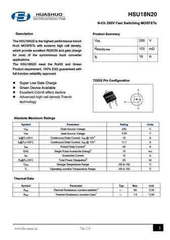
HSU18N20 N-Ch 200V Fast Switching MOSFETs Description Product Summary VDS 200 V The HSU18N20 is the highest performance trench N-ch MOSFETs with extreme high cell density, RDS(ON),max 170 m which provide excellent RDSON and gate charge for most of the synchronous buck converter ID 18 A applications. The HSU18N20 meet the RoHS and Green Product requirement, 100% EAS gua... See More ⇒
jmpc18n20bj.pdf
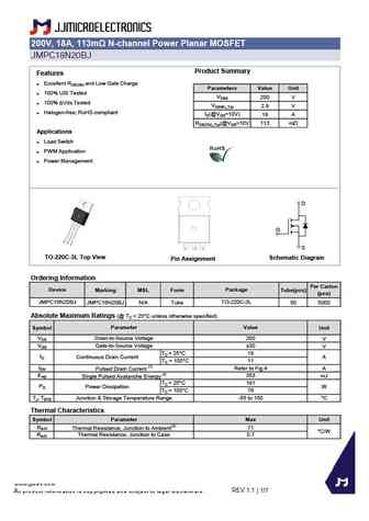
200V, 18A, 113m N-channel Power Planar MOSFET JMPC18N20BJ Product Summary Features Excellent RDS(ON) and Low Gate Charge Parameters Value Unit 100% UIS Tested VDSS 200 V 100% Vds Tested VGS(th)_Typ 2.9 V Halogen-free; RoHS-compliant ID(@VGS=10V) 18 A RDS(ON)_Typ(@VGS=10V 113 mW Applications Load Switch PWM Application Power Management D G S ... See More ⇒
jmpe18n20bj.pdf
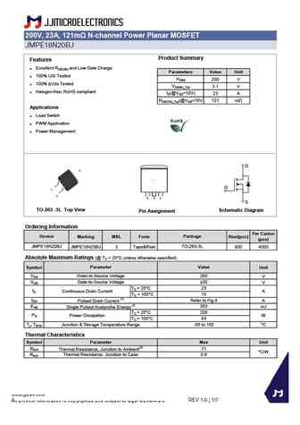
200V, 23A, 121m N-channel Power Planar MOSFET JMPE18N20BJ Product Summary Features Excellent RDS(ON) and Low Gate Charge Parameters Value Unit 100% UIS Tested VDSS 200 V 100% Vds Tested VGS(th)_Typ 3.1 V Halogen-free; RoHS-compliant ID(@VGS=10V) 23 A RDS(ON)_Typ(@VGS=10V 121 mW Applications Load Switch PWM Application Power Management D G S ... See More ⇒
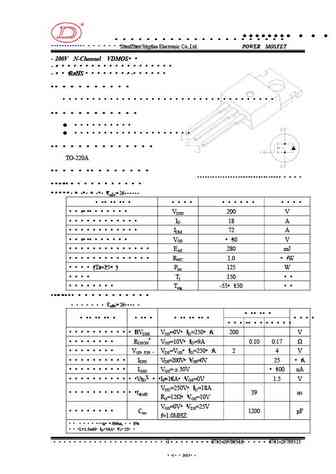
agmh18n20c.pdf
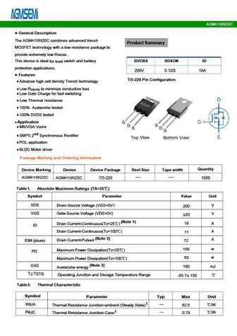
AGMH18N20C Table 3. Electrical Characteristics (TJ=25 unless otherwise noted) Symbol Parameter Conditions Min Typ Max Unit On/Off States BV Drain-Source Breakdown Voltage V =0V I =250 A -- V GS D DSS 200 -- Zero Gate Voltage Drain Current V =200V,V =0V -- 1 A DS GS I -- DSS V = 20V,V =0V -- -- nA GS DS IGSS Gate-Body Leakage Current 100 V Gate Threshold Voltage V =... See More ⇒
agm18n20h.pdf
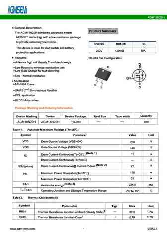
AGM18N20H General Description Product Summary The AGM18N20H combines advanced trench MOSFET technology with a low resistance package to provide extremely low R . DS(ON) BVDSS RDSON ID This device is ideal switch and battery for load 200V 120m 18A protection applications. Features TO-263 Pin Configuration Advance high cell density Trench technology D Low R to ... See More ⇒
agm18n20d.pdf
AGM18N20D Table3. Electrical Characteristics (TJ=25 unless otherwise noted) Symbol Parameter Conditions Min Typ Max Unit On/Off States BV Drain-Source Breakdown Voltage V =0V I =250 A -- V GS D DSS 200 -- Zero Gate Voltage Drain Current V =200V,V =0V -- 1 A DS GS I -- DSS V = 20V,V =0V -- -- nA GS DS IGSS Gate-Body Leakage Current 100 V Gate Threshold Voltage V =V ... See More ⇒
fqd18n20v2tm.pdf
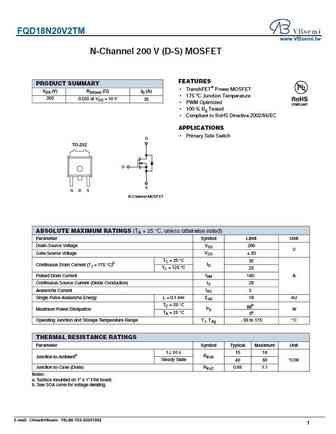
FQD18N20V2TM www.VBsemi.tw N-Channel 200 V (D-S) MOSFET FEATURES PRODUCT SUMMARY TrenchFET Power MOSFET VDS (V) RDS(on) ( )ID (A) 175 C Junction Temperature 200 0.055 at VGS = 10 V 30 PWM Optimized 100 % Rg Tested Compliant to RoHS Directive 2002/95/EC APPLICATIONS Primary Side Switch D TO-252 G S G D S N-Channel MOSFET ABSOLUTE MAXIMUM RA... See More ⇒
vbzm18n20.pdf
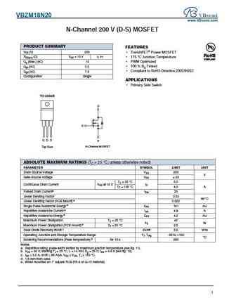
VBZM18N20 www.VBsemi.com N-Channel 200 V (D-S) MOSFET PRODUCT SUMMARY FEATURES VDS (V) 200 TrenchFET Power MOSFET RDS(on) ( )VGS = 10 V 0.91 175 C Junction Temperature Qg (Max.) (nC) 13 PWM Optimized 100 % Rg Tested Qgs (nC) 3.0 Compliant to RoHS Directive 2002/95/EC Qgd (nC) 7.9 Configuration Single APPLICATIONS Primary Side Switch TO-220AB D G... See More ⇒
fdd18n20lz.pdf
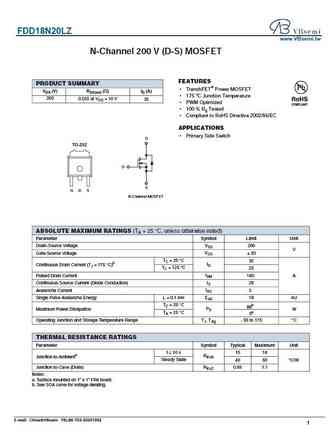
FDD18N20LZ www.VBsemi.tw N-Channel 200 V (D-S) MOSFET FEATURES PRODUCT SUMMARY TrenchFET Power MOSFET VDS (V) RDS(on) ( )ID (A) 175 C Junction Temperature 200 0.055 at VGS = 10 V 30 PWM Optimized 100 % Rg Tested Compliant to RoHS Directive 2002/95/EC APPLICATIONS Primary Side Switch D TO-252 G S G D S N-Channel MOSFET ABSOLUTE MAXIMUM RATI... See More ⇒
mdt18n20.pdf
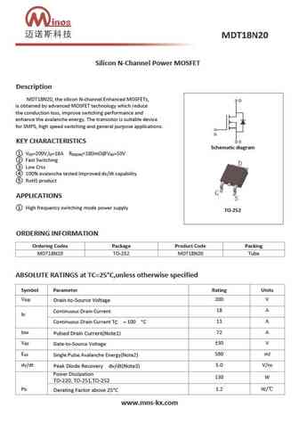
Silicon N-Channel Power MOSFET Description MDT18N20, the silicon N-channel Enhanced MOSFETs, is obtained by advanced MOSFET technology which reduce the conduction loss, improve switching performance and enhance the avalanche energy. The transistor is suitable device for SMPS, high speed switching and general purpose applications. KEY CHARACTERISTICS Schematic diagram V =200V,I =18A... See More ⇒
mp18n20 mpf18n20 mdp18n20 mdt18n20.pdf
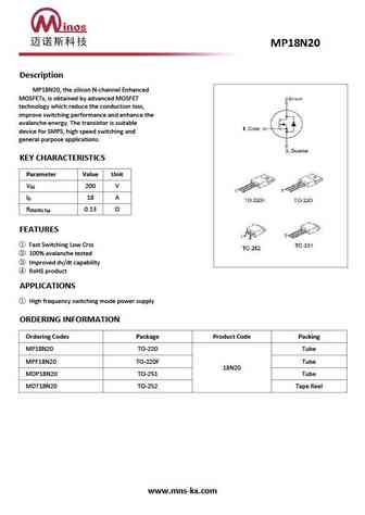
Description MP18N20, the silicon N-channel Enhanced MOSFETs, is obtained by advanced MOSFET technology which reduce the conduction loss, improve switching performance and enhance the avalanche energy. The transistor is suitable device for SMPS, high speed switching and general purpose applications. KEY CHARACTERISTICS Parameter Value Unit V 200 V DS I 18 A D R 0.13 DS(ON).Typ... See More ⇒
fxn18n20c.pdf
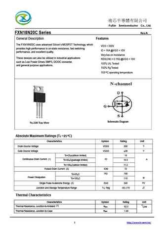
FuXin Semiconductor Co., Ltd. FXN18N20C Series Rev.A General Description Features The FXN18N20C uses advanced Silicon s MOSFET Technology, which VDS = 200V provides high performance in on-state resistance, fast switching ID = 18A @VGS = 10V performance, and excellent quality. Very low on-resistance These devices can also be utilized in indust... See More ⇒
ap18n20d ap18n20y.pdf
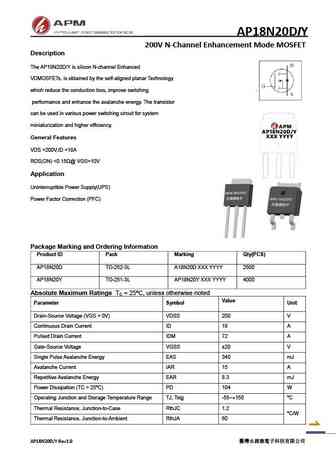
AP18N20DIY 200V N-Channel Enhancement Mode MOSFET Description The AP18N20D/Y is silicon N-channel Enhanced VDMOSFETs, is obtained by the self-aligned planar Technology which reduce the conduction loss, improve switching performance and enhance the avalanche energy. The transistor can be used in various power switching circuit for system miniaturization and higher efficiency. ... See More ⇒
Detailed specifications: 8205A, 8205B, G3205, G1010, G3710, 5N20A, 630A, 640, IRF740, 18N20A, 2N25, 3N25, 740, 840, 16N50F, 13N50F, 20N50
Keywords - 18N20 MOSFET specs
18N20 cross reference
18N20 equivalent finder
18N20 pdf lookup
18N20 substitution
18N20 replacement
Can't find your MOSFET? Learn how to find a substitute transistor by analyzing voltage, current and package compatibility
