SM3017NSU Specs and Replacement
Type Designator: SM3017NSU
Type of Transistor: MOSFET
Type of Control Channel: N-Channel
Absolute Maximum Ratings
Pd ⓘ - Maximum Power Dissipation: 50 W
|Vds|ⓘ - Maximum Drain-Source Voltage: 30 V
|Vgs|ⓘ - Maximum Gate-Source Voltage: 20 V
|Id| ⓘ - Maximum Drain Current: 68 A
Tj ⓘ - Maximum Junction Temperature: 150 °C
Electrical Characteristics
tr ⓘ - Rise Time: 12 nS
Cossⓘ - Output Capacitance: 190 pF
RDSonⓘ - Maximum Drain-Source On-State Resistance: 0.0072 Ohm
Package: TO252
SM3017NSU substitution
- MOSFET ⓘ Cross-Reference Search
SM3017NSU datasheet
sm3017nsu.pdf
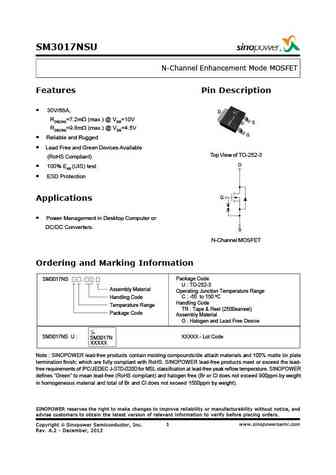
SM3017NSU N-Channel Enhancement Mode MOSFET Features Pin Description 30V/68A, D RDS(ON)=7.2m (max.) @ VGS=10V S RDS(ON)=9.8m (max.) @ VGS=4.5V G Reliable and Rugged Lead Free and Green Devices Available Top View of TO-252-3 (RoHS Compliant) D 100% EAS (UIS) test ESD Protection G Applications Power Management in Desktop Computer or DC/DC Converters. S N-Channe... See More ⇒
tsm301k12cq.pdf
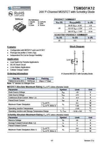
TSM301K12 20V P-Channel MOSFET with Schottky Diode TDFN 2x2 PRODUCT SUMMARY Pin Definition 1. Anode 6. Cathode VDS (V) RDS(on)(m ) ID (A) 2. NC 5. Gate 3. Drain 4. Source 94 @ VGS = -4.5V -2.8 -20 131 @ VGS = -2.5V -2.3 185 @ VGS = -1.8V -0.54 SCHOTTKY PRODUCT SUMMARY VR (V) VF (V) IF (A) 20 0.5 2 Block Diagram Features Configuration with MOSFET and L... See More ⇒
sm3016nsu.pdf

SM3016NSU N-Channel Enhancement Mode MOSFET Features Pin Description 30V/75A, D RDS(ON)=5m (Max.) @ VGS=10V S RDS(ON)=6.9m (Max.) @ VGS=4.5V G Reliable and Rugged Lead Free and Green Devices Available Top View of TO-252-3 (RoHS Compliant) ESD Protection D HBM ESD protection level pass 2KV 100% UIS + Rg Tested G Applications Power Management in Deskt... See More ⇒
gsm3016s.pdf

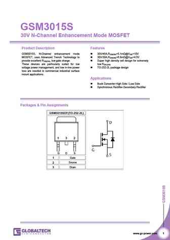
GSM3016S 30V N-Channel Enhancement Mode MOSFET Product Description Features GSM3016S, N-Channel enhancement mode 30V/45A,RDS(ON)=6m @VGS=10V MOSFET, uses Advanced Trench Technology to 30V/30A,RDS(ON)=9m @VGS=4.5V provide excellent RDS(ON), low gate charge. Super high density cell design for extremely These devices are particularly suited for low low RDS (ON) voltag... See More ⇒

Detailed specifications: SM4373NAKP, SM4373NSKP, SM4374NSKP, SM2F04NSU, SM2F05NSU, SM2F07NSU, SM3005NAF, SM3016NSU, IRFP250, SM3023NSU, SM3023NSV, SM3116NAU, SM3116NSUC, SM4375NSKP, SM4377NSKP, SM4378NSKP, SM4383NSKP
Keywords - SM3017NSU MOSFET specs
SM3017NSU cross reference
SM3017NSU equivalent finder
SM3017NSU pdf lookup
SM3017NSU substitution
SM3017NSU replacement
Learn how to find the right MOSFET substitute. A guide to cross-reference, check specs and replace MOSFETs in your circuits.
History: AM3441P | AM30N03-40D
🌐 : EN ES РУ

LIST
Last Update
MOSFET: FTF30P35D | FTF25N35DHVT | FTF15N35D | FTE15C35G | FTP02P15G | FTE02P15G | AKF30N5P0SX | AKF30N10S | AKF20P45D | CM4407
Popular searches
2n5088 datasheet | irfp064n | tip31 transistor | 2sc1384 | mj21196g | irfb4115 | 21270 transistor | k3569