IPD050N03L Specs and Replacement
Type Designator: IPD050N03L
Type of Transistor: MOSFET
Type of Control Channel: N-Channel
Absolute Maximum Ratings
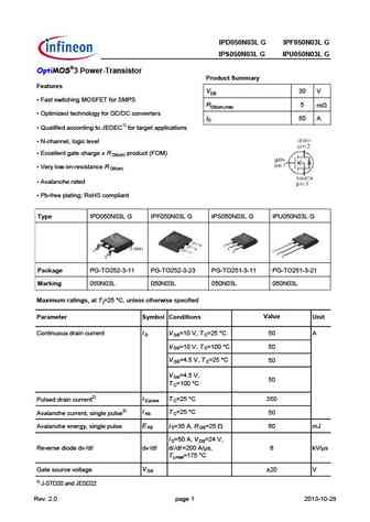
Pd ⓘ - Maximum Power Dissipation: 68 W
|Vds|ⓘ - Maximum Drain-Source Voltage: 30 V
|Vgs|ⓘ - Maximum Gate-Source Voltage: 20 V
|Id| ⓘ - Maximum Drain Current: 50 A
Tj ⓘ - Maximum Junction Temperature: 175 °C
Electrical Characteristics
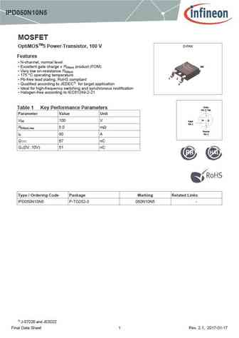
tr ⓘ - Rise Time: 13 nS
Cossⓘ - Output Capacitance: 920 pF
RDSonⓘ - Maximum Drain-Source On-State Resistance: 0.005 Ohm
Package: TO-252
IPD050N03L substitution
- MOSFET ⓘ Cross-Reference Search
IPD050N03L datasheet
ipd050n03lg ipf050n03lg ips050n03lg ipu050n03lg ipd050n03l ips050n03l.pdf
Type IPD050N03L G IPF050N03L G IPS050N03L G IPU050N03L G OptiMOS 3 Power-Transistor Product Summary Features VDS 30 V Fast switching MOSFET for SMPS RDS(on),max 5 mW Optimized technology for DC/DC converters ID 50 A Qualified according to JEDEC1) for target applications N-channel, logic level Excellent gate charge x R product (FOM) DS(on) Very low on... See More ⇒
ipd050n03l ipf050n03l ips050n03l ipu050n03l.pdf
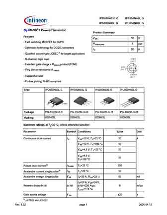
Type IPD050N03L G IPF050N03L G IPS050N03L G IPU050N03L G OptiMOS 3 Power-Transistor Product Summary Features V 30 V DS Fast switching MOSFET for SMPS R 5 m DS(on),max Optimized technology for DC/DC converters I 50 A D Qualified according to JEDEC1) for target applications N-channel, logic level Excellent gate charge x R product (FOM) DS(on) Very low... See More ⇒
ipd050n03l.pdf
isc N-Channel MOSFET Transistor IPD050N03L, IIPD050N03L FEATURES Static drain-source on-resistance RDS(on) 5m Enhancement mode 100% avalanche tested Minimum Lot-to-Lot variations for robust device performance and reliable operation DESCRITION Fast switching ABSOLUTE MAXIMUM RATINGS(T =25 ) a SYMBOL PARAMETER VALUE UNIT V Drain-Source Voltage 30 V DSS V Ga... See More ⇒
ipd050n03lg.pdf
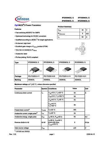
pe % # ! % # ! %' # ! %) # ! % (>.;?6?@ %>E Features D R 3DE DH;E5 ;@9 ') - . 8AC -'*- m D n) m x R ) BE;?;K76 E75 @A>A9J 8AC 5A@G7CE7CD D 1) R + F3>;8;76 355AC6;@9 EA $ 8AC E3C97E 3BB>;53E;A@D R ( 5 3@@7> >A9;5 >7G7> R I57>>7@E 93E7 5 3C97 I BCA6F5E ) ' D n) R 07CJ >AH A@ C7D;DE3@57 D n) R G3>3@5 7 C3E76 R *4 8C77 B>3E;@9 , A"- 5A?B>;3@E Type... See More ⇒
Detailed specifications: IPD50R1K4CE, IPD13N03LAG, IPD135N03L, IPD090N03L, IPD075N03L, IPD06N03LBG, IPD060N03L, IPD053N06N, K3569, IPD04N03LBG, IPD040N03L, IPD03N03LAG, IPD031N03L, IPD025N06N, IPD024N06N, IPB90R340C3, IPB80N06S3L-05
Keywords - IPD050N03L MOSFET specs
IPD050N03L cross reference
IPD050N03L equivalent finder
IPD050N03L pdf lookup
IPD050N03L substitution
IPD050N03L replacement
Need a MOSFET replacement? Our guide shows you how to find a perfect substitute by comparing key parameters and specs
History: IPB65R095C7 | HSS2607 | IPB80P04P4-07 | IPD025N06N
🌐 : EN ES РУ
LIST
Last Update
MOSFET: AUP060N055 | AUP056N10 | AUP056N08BGL | AUP052N085 | AUP045N12 | AUP039N10 | AUP034N10 | AUP034N06 | AUP033N08BG | AUP026N085
Popular searches
k117 transistor | 2sc2291 | bc139 | 2sc1398 | 2sd218 | bc547 характеристики | me15n10-g | 2n2905 equivalent


