IPB020N10N5 Specs and Replacement
Type Designator: IPB020N10N5
Type of Transistor: MOSFET
Type of Control Channel: N-Channel
Absolute Maximum Ratings
Pd ⓘ - Maximum Power Dissipation: 375 W
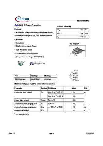
|Vds|ⓘ - Maximum Drain-Source Voltage: 100 V
|Vgs|ⓘ - Maximum Gate-Source Voltage: 20 V
|Id| ⓘ - Maximum Drain Current: 120 A
Tj ⓘ - Maximum Junction Temperature: 175 °C
Electrical Characteristics
tr ⓘ - Rise Time: 26 nS
Cossⓘ - Output Capacitance: 1810 pF
RDSonⓘ - Maximum Drain-Source On-State Resistance: 0.002 Ohm
Package: TO-263
IPB020N10N5 substitution
- MOSFET ⓘ Cross-Reference Search
IPB020N10N5 datasheet
ipb020n10n5.pdf

MOSFET Metal Oxide Semiconductor Field Effect Transistor OptiMOSTM OptiMOS 5 Power-Transistor, 100 V IPB020N10N5 Data Sheet Rev. 2.1 Final Power Management & Multimarket OptiMOS 5 Power-Transistor, 100 V IPB020N10N5 D PAK 1 Description Features N-channel, normal level Optimized for FOM OSS Very low on-resistance R DS(on) 175 C operating temperature ... See More ⇒
ipb020n10n5.pdf
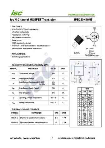
INCHANGE Semiconductor isc N-Channel MOSFET Transistor IPB020N10N5 FEATURES With TO-263(D2PAK) packaging Ultra-fast body diode High speed switching Very low on-resistence Easy to use 100% avalanche tested Minimum Lot-to-Lot variations for robust device performance and reliable operationz APPLICATIONS Switching applications ABSOLUTE MAXIMUM RATINGS(T =25 ) a... See More ⇒
ipb020n10n5lf.pdf
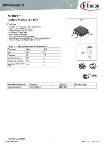
IPB020N10N5LF MOSFET D PAK OptiMOSTM 5 Linear FET, 100 V Features Ideal for hot-swap and e-fuse applications Very low on-resistance R DS(on) Wide safe operating area SOA N-channel, normal level 100% avalanche tested Pb-free plating; RoHS compliant Qualified according to JEDEC1) for target applications Halogen-free according to IEC61249-2-21 Drain ... See More ⇒
ipb020n10n5lf.pdf
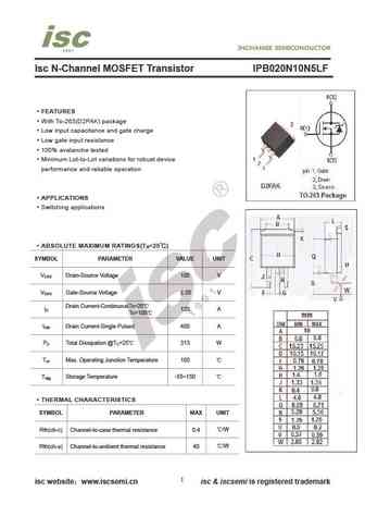
Isc N-Channel MOSFET Transistor IPB020N10N5LF FEATURES With To-263(D2PAK) package Low input capacitance and gate charge Low gate input resistance 100% avalanche tested Minimum Lot-to-Lot variations for robust device performance and reliable operation APPLICATIONS Switching applications ABSOLUTE MAXIMUM RATINGS(T =25 ) a SYMBOL PARAMETER VALUE UNIT V Drain-Source... See More ⇒
Detailed specifications: IPB03N03LBG, IPB039N10N3GE8187, IPB034N03L, IPB031N08N5, IPB029N06N3GE8187, IPB027N10N5, IPB026N06N, IPB024N08N5, AO4468, IPB020N08N5, IPB017N10N5, IPB017N08N5, IPB015N08N5, IPB015N04L, IPB014N06N, IPB011N04L, IPB010N06N
Keywords - IPB020N10N5 MOSFET specs
IPB020N10N5 cross reference
IPB020N10N5 equivalent finder
IPB020N10N5 pdf lookup
IPB020N10N5 substitution
IPB020N10N5 replacement
Can't find your MOSFET? Learn how to find a substitute transistor by analyzing voltage, current and package compatibility
History: IRF630N | IRFP4242PBF | IPD50R950CE | TMU8N60H | FQB8N60CFTM | FQD13N10TM | TMC8N65H
🌐 : EN ES РУ

LIST
Last Update
MOSFET: AUP060N055 | AUP056N10 | AUP056N08BGL | AUP052N085 | AUP045N12 | AUP039N10 | AUP034N10 | AUP034N06 | AUP033N08BG | AUP026N085
Popular searches
fgpf4636 datasheet | 2sc1945 | c2383 | 2sb681 | bc639 equivalent | bd138 transistor equivalent | c1096 transistor | c1345 transistor