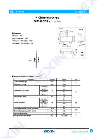
SI2316DS Specs and Replacement
Type Designator: SI2316DS
Type of Transistor: MOSFET
Type of Control Channel: N-Channel
Absolute Maximum Ratings
Pd ⓘ - Maximum Power Dissipation: 0.7 W
|Vds|ⓘ - Maximum Drain-Source Voltage: 30 V
|Vgs|ⓘ - Maximum Gate-Source Voltage: 20 V
|Id| ⓘ - Maximum Drain Current: 2.9 A
Tj ⓘ - Maximum Junction Temperature: 150 °C
Electrical Characteristics
tr ⓘ - Rise Time: 9 nS
Cossⓘ - Output Capacitance: 90 pF
RDSonⓘ - Maximum Drain-Source On-State Resistance: 0.05 Ohm
Package: SOT-23
SI2316DS substitution
- MOSFET ⓘ Cross-Reference Search
SI2316DS datasheet
si2316ds.pdf

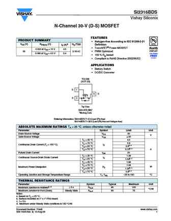
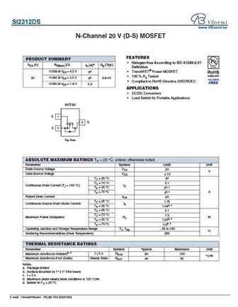
Si2316DS Vishay Siliconix N-Channel 30-V (D-S) MOSFET FEATURES PRODUCT SUMMARY Halogen-free Option Available VDS (V) RDS(on) ( )ID (A) Pb-free TrenchFET Power MOSFET 0.050 at VGS = 10 V 3.4 Available 30 0.085 at VGS = 4.5 V 2.6 RoHS* APPLICATIONS COMPLIANT Battery Switch TO-236 (SOT-23) G 1 3 D S 2 Top View Si2316DS (C6)* * Marking Code Ordering I... See More ⇒
si2316bd.pdf

Si2316BDS Vishay Siliconix N-Channel 30-V (D-S) MOSFET FEATURES PRODUCT SUMMARY Halogen-free According to IEC 61249-2-21 VDS (V) RDS(on) ( ) ID (A)a Qg (Typ) Definition TrenchFET Power MOSFET 0.050 at VGS = 10 V 4.5 30 3.16 nC PWM Optimized 0.080 at VGS = 4.5 V 3.4 100 % Rg tested Compliant to RoHS Directive 2002/95/EC APPLICATIONS Battery Switch... See More ⇒
si2316bds.pdf
Si2316BDS Vishay Siliconix N-Channel 30-V (D-S) MOSFET FEATURES PRODUCT SUMMARY Halogen-free According to IEC 61249-2-21 VDS (V) RDS(on) ( ) ID (A)a Qg (Typ) Definition TrenchFET Power MOSFET 0.050 at VGS = 10 V 4.5 30 3.16 nC PWM Optimized 0.080 at VGS = 4.5 V 3.4 100 % Rg tested Compliant to RoHS Directive 2002/95/EC APPLICATIONS Battery Switch... See More ⇒
si2319cd.pdf
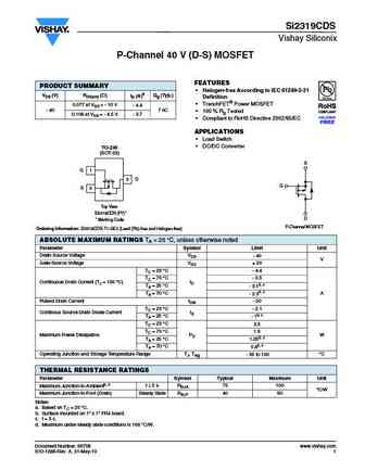
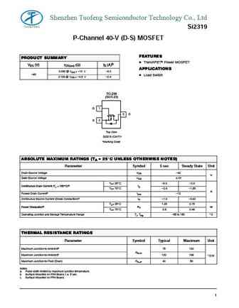
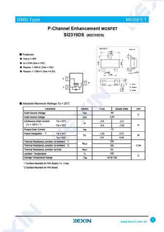
Si2319CDS Vishay Siliconix P-Channel 40 V (D-S) MOSFET FEATURES PRODUCT SUMMARY Halogen-free According to IEC 61249-2-21 VDS (V) RDS(on) ( ) ID (A)a Qg (Typ.) Definition TrenchFET Power MOSFET 0.077 at VGS = - 10 V - 4.4 - 40 7 nC 100 % Rg Tested 0.108 at VGS = - 4.5 V - 3.7 Compliant to RoHS Directive 2002/95/EC APPLICATIONS Load Switch DC/DC ... See More ⇒
si2318cd.pdf

New Product Si2318CDS Vishay Siliconix N-Channel 40 V (D-S) MOSFET FEATURES PRODUCT SUMMARY Halogen-free According to IEC 61249-2-21 VDS (V) RDS(on) ( ) ID (A)a Qg (Typ.) Definition 0.042 at VGS = 10 V TrenchFET Power MOSFET 5.6 40 2.9 nC 100 % Rg Tested 0.051 at VGS = 4.5 V 5.1 Compliant to RoHS Directive 2002/95/EC APPLICATIONS DC/DC Converte... See More ⇒
si2319cds.pdf

Si2319CDS Vishay Siliconix P-Channel 40 V (D-S) MOSFET FEATURES PRODUCT SUMMARY Halogen-free According to IEC 61249-2-21 VDS (V) RDS(on) ( ) ID (A)a Qg (Typ.) Definition TrenchFET Power MOSFET 0.077 at VGS = - 10 V - 4.4 - 40 7 nC 100 % Rg Tested 0.108 at VGS = - 4.5 V - 3.7 Compliant to RoHS Directive 2002/95/EC APPLICATIONS Load Switch DC/DC ... See More ⇒
si2312cds.pdf
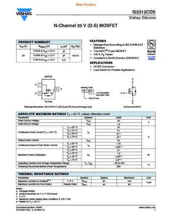
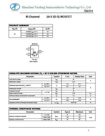
New Product Si2312CDS Vishay Siliconix N-Channel 20 V (D-S) MOSFET FEATURES PRODUCT SUMMARY Halogen-free According to IEC 61249-2-21 VDS (V) RDS(on) ( ) ID (A)e Qg (Typ.) Definition 0.0318 at VGS = 4.5 V TrenchFET Power MOSFET 6a 100 % Rg Tested 20 0.0356 at VGS = 2.5 V 6a 8.8 nC Compliant to RoHS Directive 2002/95/EC 0.0414 at VGS = 1.8 V 5.6 APPLI... See More ⇒
si2319ds.pdf
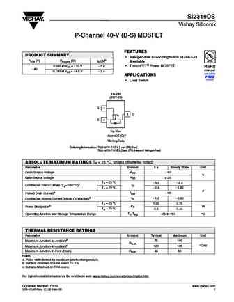
Si2319DS Vishay Siliconix P-Channel 40-V (D-S) MOSFET FEATURES PRODUCT SUMMARY Halogen-free According to IEC 61249-2-21 VDS (V) RDS(on) ( ) ID (A)b Available 0.082 at VGS = - 10 V TrenchFET Power MOSFET - 3.0 - 40 0.130 at VGS = - 4.5 V - 2.4 APPLICATIONS Load Switch TO-236 (SOT-23) G 1 3 D S 2 Top View Si2319DS (C9)* *Marking Code Ordering Informati... See More ⇒
si2314ed.pdf
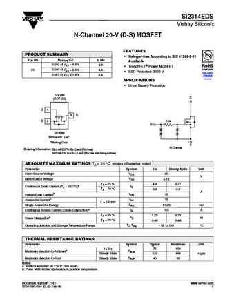
Si2314EDS Vishay Siliconix N-Channel 20-V (D-S) MOSFET FEATURES PRODUCT SUMMARY Halogen-free According to IEC 61249-2-21 VDS (V) RDS(on) ( )ID (A) Available 0.033 at VGS = 4.5 V 4.9 TrenchFET Power MOSFET 0.040 at VGS = 2.5 V 20 4.4 ESD Protected 3000 V 0.051 at VGS = 1.8 V 3.9 APPLICATIONS LI-lon Battery Protection TO-236 D (SOT-23) G 1 3 D 3... See More ⇒
si2315bds.pdf
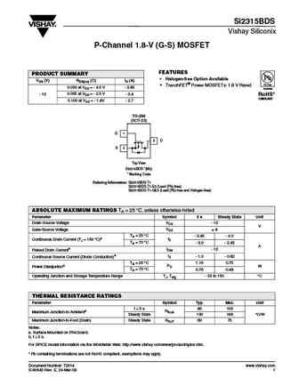
Si2315BDS Vishay Siliconix P-Channel 1.8-V (G-S) MOSFET FEATURES PRODUCT SUMMARY Halogen-free Option Available VDS (V) RDS(on) ( )ID (A) Pb-free TrenchFET Power MOSFETs 1.8 V Rated 0.050 at VGS = - 4.5 V - 3.85 Available 0.065 at VGS = - 2.5 V - 12 - 3.4 RoHS* COMPLIANT 0.100 at VGS = - 1.8V - 2.7 TO-236 (SOT-23) G 1 3 D S 2 Top View Si2315BDS *(M5) *... See More ⇒
si2312bds.pdf
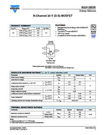
Si2312BDS Vishay Siliconix N-Channel 20 V (D-S) MOSFET FEATURES PRODUCT SUMMARY Halogen-free According to IEC 61249-2-21 VDS (V) RDS(on) ( )ID (A) Qg (Typ.) Definition 0.031 at VGS = 4.5 V 5.0 TrenchFET Power MOSFET 20 0.037 at VGS = 2.5 V 4.6 7.5 100 % Rg Tested 0.047 at VGS = 1.8 V 4.1 Compliant to RoHS Directive 2002/95/EC TO-236 (SOT-23) G 1 3 D S 2... See More ⇒
si2318ds.pdf
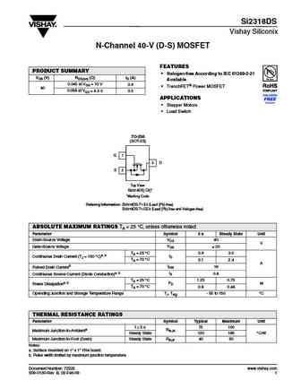
Si2318DS Vishay Siliconix N-Channel 40-V (D-S) MOSFET FEATURES PRODUCT SUMMARY Halogen-free According to IEC 61249-2-21 VDS (V) RDS(on) ( )ID (A) Available 0.045 at VGS = 10 V 3.9 TrenchFET Power MOSFET 40 0.058 at VGS = 4.5 V 3.5 APPLICATIONS Stepper Motors Load Switch TO-236 (SOT-23) G 1 3 D S 2 Top View Si2318DS( C8)* *Marking Code Ordering... See More ⇒
si2314eds.pdf
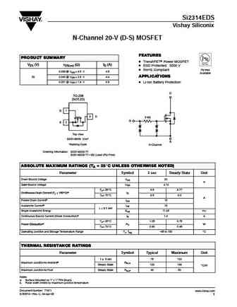
Si2314EDS Vishay Siliconix N-Channel 20-V (D-S) MOSFET FEATURES PRODUCT SUMMARY D TrenchFETr Power MOSFET VDS (V) rDS(on) (W) ID (A) D ESD Protected 3000 V D RoHS Compliant Pb-free 0.033 @ VGS = 4.5 V 4.9 Available APPLICATIONS 0.040 @ VGS = 2.5 V 4.4 20 0.051 @ VGS = 1.8 V 3.9 D LI-lon Battery Protection D TO-236 (SOT-23) G 1 3 D 3 kW G S 2 Top View Si2314EDS (C4)* S... See More ⇒
si2318cds.pdf
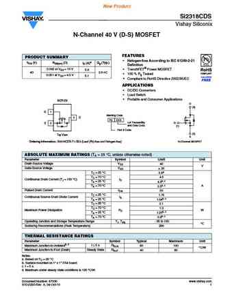
New Product Si2318CDS Vishay Siliconix N-Channel 40 V (D-S) MOSFET FEATURES PRODUCT SUMMARY Halogen-free According to IEC 61249-2-21 VDS (V) RDS(on) ( ) ID (A)a Qg (Typ.) Definition 0.042 at VGS = 10 V TrenchFET Power MOSFET 5.6 40 2.9 nC 100 % Rg Tested 0.051 at VGS = 4.5 V 5.1 Compliant to RoHS Directive 2002/95/EC APPLICATIONS DC/DC Converte... See More ⇒
si2311ds.pdf
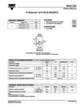
Si2311DS Vishay Siliconix P-Channel 1.8-V (G-S) MOSFET FEATURES PRODUCT SUMMARY Halogen-free Option Available VDS (V) RDS(on) ( )ID (A) TrenchFET Power MOSFET 0.045 at VGS = - 4.5 V - 3.5 RoHS 0.072 at VGS = - 2.5 V - 8 - 2.8 COMPLIANT APPLICATIONS 0.120 at VGS = - 1.8 V - 2.0 Load Switch TO-236 (SOT-23) G 1 3 D S 2 Top View Si2311DS (C1)* * Marki... See More ⇒
si2312ds.pdf
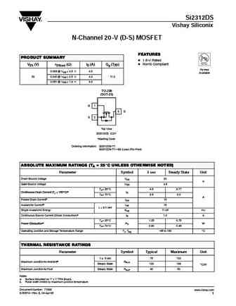
Si2312DS Vishay Siliconix N-Channel 20 -V (D-S) MOSFET FEATURES PRODUCT SUMMARY D 1.8-V Rated D RoHS Compliant VDS (V) rDS(on) (W) ID (A) Qg (Typ) Pb-free 0.033 @ VGS = 4.5 V 4.9 Available 0.040 @ VGS = 2.5 V 4.4 20 11.2 0.051 @ VGS = 1.8 V 3.9 TO-236 (SOT-23) G 1 3 D S 2 Top View Si2312DS (C2)* *Marking Code Ordering Information Si2312DS-T1 Si2312DS-T1 E3 (Lead (Pb)-F... See More ⇒
si2310b.pdf
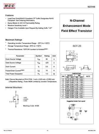
SI2310B Features Lead Free Finish/RoHS Compliant ("P" Suffix Designates RoHS Compliant. See Ordering Information) N-Channel Epoxy Meets UL 94 V-0 Flammability Rating Moisture Sensitivity Level 1 Enhancement Mode Halogen Free Available Upon Request By Adding Suffix "-HF" Field Effect Transistor Maximum Ratings Operating Junction Temperature Range -55 C to +150... See More ⇒
si2310a.pdf
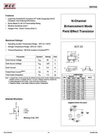
SI2310A Features Lead Free Finish/RoHS Compliant ("P" Suffix Designates RoHS Compliant. See Ordering Information) N-Channel Epoxy Meets UL 94 V-0 Flammability Rating Moisture Sensitivity Level 1 Enhancement Mode Halogen Free. Green Device (Note 1) Field Effect Transistor Maximum Ratings Operating Junction Temperature Range -55 C to +150 C Storage ... See More ⇒
si2310.pdf
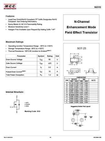
SI2310 Features Lead Free Finish/RoHS Compliant ("P" Suffix Designates RoHS Compliant. See Ordering Information) N-Channel Epoxy Meets UL 94 V-0 Flammability Rating Moisture Sensitivity Level 1 Enhancement Mode Halogen Free Available Upon Request By Adding Suffix "-HF" Field Effect Transistor Maximum Ratings Operating Junction Temperature Range -55 C to +150 ... See More ⇒
si2312.pdf
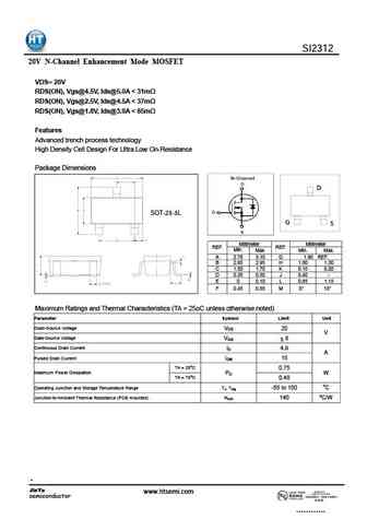
SI2312 20V N-Channel Enhancement Mode MOSFET VDS= 20V RDS(ON), Vgs@4.5V, Ids@5.0A ... See More ⇒
si2315.pdf
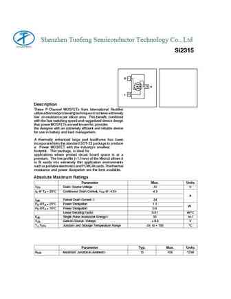
Shenzhen Tuofeng Semiconductor Technology Co., Ltd Si2315 G 1 3 D S 2 Description These P-Channel MOSFETs from International Rectifier utilize advanced processing techniques to achieve extremely low on-resistance per silicon area. This benefit, combined with the fast switching speed and ruggedized device design that power MOSFETs are well known for, provides the designer with an ext... See More ⇒
si2312.pdf
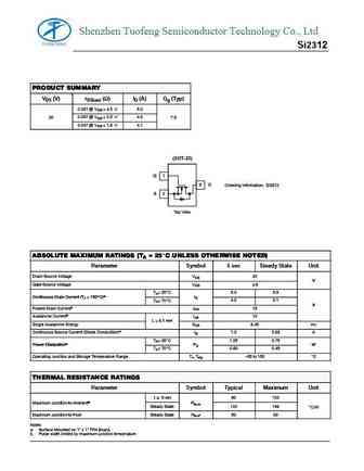
Shenzhen Tuofeng Semiconductor Technology Co., Ltd Si2312 PRODUCT SUMMARY VDS (V) rDS(on) (W) ID (A) Qg (Typ) 0.031 @ VGS = 4.5 V 5.0 0.037 @ VGS = 2.5 V 4.6 20 7.5 0.047 @ VGS = 1.8 V 4.1 (SOT-23) G 1 3 D Ordering Information Si2312 S 2 Top View ABSOLUTE MAXIMUM RATINGS (TA = 25_C UNLESS OTHERWISE NOTED) Parameter Symbol 5 sec Steady State Unit Drain-Source Voltage VDS 20 V ... See More ⇒
si2310.pdf
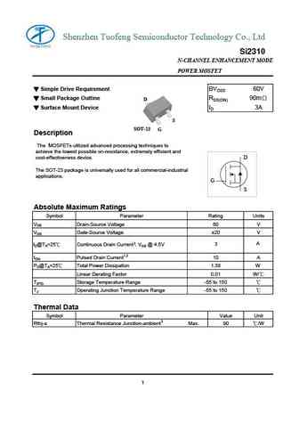
Shenzhen Tuofeng Semiconductor Technology Co., Ltd Si2310 N-CHANNEL ENHANCEMENT MODE POWER MOSFET Simple Drive Requirement BVDSS 60V Small Package Outline RDS(ON) 90m D Surface Mount Device ID 3A S SOT-23 G Description The MOSFETs utilized advanced processing techniques to achieve the lowest possible on-resistance,... See More ⇒
si2319.pdf
Shenzhen Tuofeng Semiconductor Technology Co., Ltd Si2319 P-Channel 40-V (D-S) MOSFET FEATURES PRODUCT SUMMARY D TrenchFETr Power MOSFET VDS (V) rDS(on) (W) ID (A)b APPLICATIONS 0.082 @ VGS = -10 V -3.0 -40 40 D Load Switch 0.130 @ VGS = -4.5 V -2.4 TO-236 (SOT-23) G 1 3 D S 2 Top View Si2319 (C91T)* *Marking Code ABSOLUTE MAXIMUM RATINGS (TA = 25_C UNLESS OTHERWISE NOTED)... See More ⇒
si2314.pdf
Shenzhen Tuofeng Semiconductor Technology Co., Ltd Si2314 N-Channel 20-V (D-S) MOSFET PRODUCT SUMMARY VDS (V) rDS(on) (W) ID (A) 0.033 @ VGS = 4.5 V 4.9 0.040 @ VGS = 2.5 V 4.4 20 0.051 @ VGS = 1.8 V 3.9 (SOT-23) G 1 3 D S 2 Top View Si2314 (AEXT) ABSOLUTE MAXIMUM RATINGS (TA = 25_C UNLESS OTHERWISE NOTED) Parameter Symbol 5 sec Steady State Unit Drain-Source Voltage VDS 20 V... See More ⇒
si2318ds-3.pdf
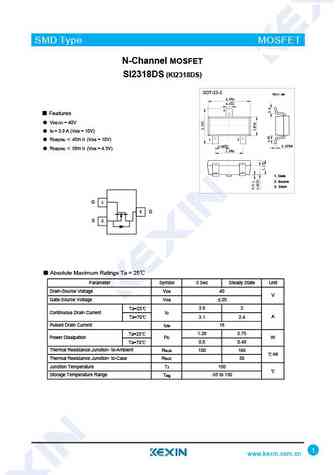
SMD Type MOSFET N-Channel MOSFET SI2318DS (KI2318DS) SOT-23-3 Unit mm +0.2 2.9 -0.1 +0.1 0.4 -0.1 3 Features VDS (V) = 40V ID = 3.9 A (VGS = 10V) 1 2 RDS(ON) 45m (VGS = 10V) +0.02 +0.1 0.15 -0.02 0.95 -0.1 RDS(ON) 58m (VGS = 4.5V) +0.1 1.9 -0.2 1. Gate 2. Source 3. Drain G 1 3 D S 2 Absolute Maximum Ratings Ta = 25 Paramet... See More ⇒
si2312ds-3.pdf
SMD Type MOSFET N-Channel Enhancement MOSFET SI2312DS (KI2312DS) SOT-23-3 Unit mm +0.2 2.9-0.1 +0.1 0.4 -0.1 Features 3 VDS (V) = 20V ID = 4.9 A (VGS =4.5V) RDS(ON) 33m (VGS = 4.5V) 1 2 RDS(ON) 40m (VGS = 2.5V) +0.02 +0.1 0.15 -0.02 0.95 -0.1 +0.1 1.9 -0.2 RDS(ON) 51m (VGS = 1.8V) G 1 3 D 1. Gate 2. Source S 2 3. Drain... See More ⇒
si2319ds.pdf
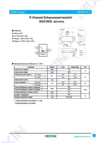
SMD Type MOSFET P-Channel Enhancement MOSFET SI2319DS (KI2319DS) SOT-23 Unit mm Features +0.1 2.9-0.1 +0.1 0.4 -0.1 VDS (V) =-40V 3 ID =-3.0A (VGS =-10V) RDS(ON) 82m (VGS =-10V) RDS(ON) 130m (VGS =-4.5V) 1 2 +0.1 +0.05 0.95 -0.1 0.1 -0.01 1.9+0.1 -0.1 G 1 3 D 1.Gate 2.Source S 2 3.Drain Absolute Maximum Ratings Ta = 25 Par... See More ⇒
si2312 ki2312.pdf
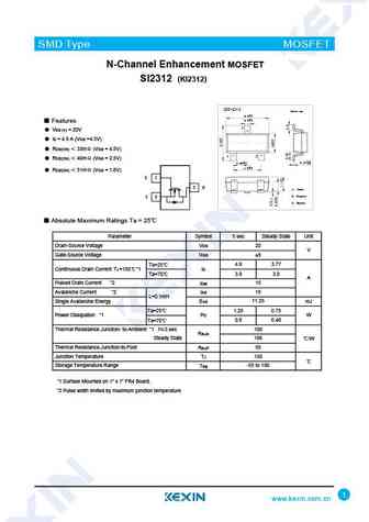
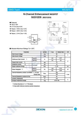
SMD Type MOSFET N-Channel Enhancement MOSFET SI2312 (KI2312) SOT-23-3 Unit mm +0.2 2.9-0.1 +0.1 0.4 -0.1 Features 3 VDS (V) = 20V ID = 4.9 A (VGS =4.5V) RDS(ON) 33m (VGS = 4.5V) 1 2 RDS(ON) 40m (VGS = 2.5V) +0.02 +0.1 0.15 -0.02 0.95 -0.1 +0.1 1.9 -0.2 RDS(ON) 51m (VGS = 1.8V) G 1 3 D 1. Gate 2. Source S 2 3. Drain Abs... See More ⇒
si2315bds.pdf
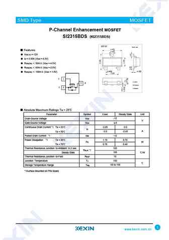
SMD Type MOSFET P-Channel Enhancement MOSFET SI2315BDS (KI2315BDS) SOT-23 Unit mm +0.1 2.9 -0.1 Features +0.1 0.4 -0.1 VDS (V) =-12V 3 ID =-3.85A (VGS =-4.5V) RDS(ON) 50m (VGS =-4.5V) RDS(ON) 65m (VGS =-2.5V) 1 2 +0.1 +0.05 0.95-0.1 0.1-0.01 RDS(ON) 100m (VGS =-1.8V) +0.1 1.9-0.1 G 1 1.Gate 3 D 2.Source S 2 3.Drain A... See More ⇒
si2318ds.pdf

SMD Type MOSFET N-Channel MOSFET SI2318DS (KI2318DS) SOT-23 Unit mm +0.1 2.9 -0.1 +0.1 0.4 -0.1 3 Features VDS (V) = 40V ID = 3.9 A (VGS = 10V) RDS(ON) 45m (VGS = 10V) 1 2 +0.1 +0.05 0.95 -0.1 RDS(ON) 58m (VGS = 4.5V) 0.1-0.01 +0.1 1.9 -0.1 1. Gate 2. Source 3. Drain G 1 3 D S 2 Absolute Maximum Ratings Ta = 25 Parameter Sy... See More ⇒
si2314eds.pdf
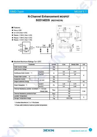
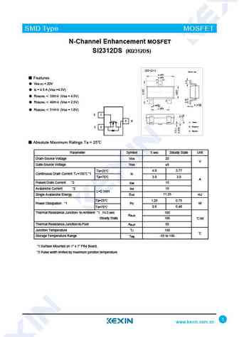
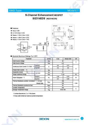
SMD Type MOSFET N-Channel Enhancement MOSFET SI2314EDS (KI2314EDS) SOT-23 Unit mm +0.1 2.9 -0.1 Features +0.1 0.4-0.1 VDS (V) = 20V 3 ID = 4.9 A (VGS = 4.5V) RDS(ON) 33m (VGS = 4.5V) RDS(ON) 40m (VGS = 2.5V) 1 2 D +0.1 +0.05 RDS(ON) 51m (VGS = 1.8V) 0.95 -0.1 0.1 -0.01 +0.1 1.9-0.1 G 1 3 k 1.Gate G 3 D 2.Source 3.Drai... See More ⇒
si2318cds.pdf
SMD Type MOSFET N-Channel MOSFET SI2318CDS (KI2318CDS) SOT-23 Unit mm +0.1 2.9 -0.1 +0.1 0.4 -0.1 Features 3 VDS (V) = 40V ID = 5.6 A (VGS = 10V) RDS(ON) 42m (VGS = 10V) 1 2 RDS(ON) 51m (VGS = 4.5V) +0.1 +0.05 0.95 -0.1 0.1 -0.01 +0.1 1.9-0.1 D 1. Gate 2. Source 3. Drain G S Absolute Maximum Ratings Ta = 25 Parameter Symbol... See More ⇒
si2318cds-3.pdf
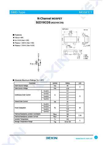
SMD Type MOSFET N-Channel MOSFET SI2318CDS (KI2318CDS) SOT-23-3 Unit mm +0.2 2.9 -0.1 +0.1 0.4 -0.1 3 Features VDS (V) = 40V ID = 5.6 A (VGS = 10V) RDS(ON) 42m (VGS = 10V) 1 2 +0.02 +0.1 0.15 -0.02 RDS(ON) 51m (VGS = 4.5V) 0.95 -0.1 +0.1 1.9 -0.2 D 1. Gate 2. Source 3. Drain G S Absolute Maximum Ratings Ta = 25 Parameter Sy... See More ⇒
si2315bds-3.pdf
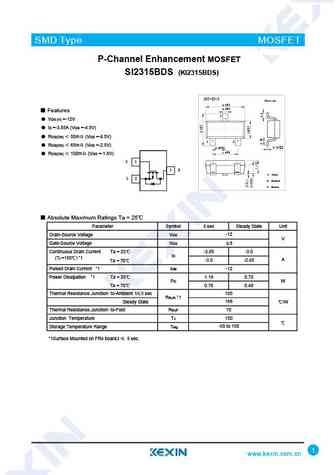
SMD Type MOSFET P-Channel Enhancement MOSFET SI2315BDS (KI2315BDS) SOT-23-3 Unit mm +0.2 2.9 -0.1 +0.1 0.4-0.1 Features 3 VDS (V) =-12V ID =-3.85A (VGS =-4.5V) RDS(ON) 50m (VGS =-4.5V) 1 2 RDS(ON) 65m (VGS =-2.5V) +0.02 +0.1 0.15 -0.02 0.95 -0.1 +0.1 1.9 -0.2 RDS(ON) 100m (VGS =-1.8V) G 1 3 D 1. Gate S 2 2. Source 3. D... See More ⇒
si2314eds-3.pdf
SMD Type MOSFET N-Channel Enhancement MOSFET SI2314EDS (KI2314EDS) SOT-23-3 Unit mm +0.2 2.9 -0.1 +0.1 Features 0.4-0.1 3 VDS (V) = 20V ID = 4.9 A (VGS = 4.5V) RDS(ON) 33m (VGS = 4.5V) 1 2 RDS(ON) 40m (VGS = 2.5V) D +0.02 +0.1 0.15 -0.02 0.95 -0.1 RDS(ON) 51m (VGS = 1.8V) +0.1 1.9 -0.2 3 k G G 1 1. Gate 2. Source 3 D 3.... See More ⇒
si2312ds.pdf
SMD Type MOSFET N-Channel Enhancement MOSFET SI2312DS (KI2312DS) SOT-23 Unit mm Features +0.1 2.9-0.1 +0.1 0.4 -0.1 VDS (V) = 20V 3 ID = 4.9 A (VGS =4.5V) RDS(ON) 33m (VGS = 4.5V) RDS(ON) 40m (VGS = 2.5V) 1 2 RDS(ON) 51m (VGS = 1.8V) +0.1 +0.05 0.95 -0.1 0.1 -0.01 1.9+0.1 -0.1 G 1 1.Gate 3 D 2.Source S 2 3.Drain Abs... See More ⇒
si2318a.pdf
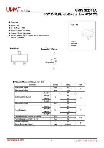
R UMW UMW SI2318A SOT-23-3L Plastic-Encapsulate MOSFETS Features SOT 23 VDS (V) = 40V ID = 5.6 A (VGS = 10V) RDS(ON) 42m (VGS = 10V) RDS(ON) 51m (VGS = 4.5V) Pb-Free Package May be Available. The G-Suffix Denotes a Pb-Free Lead Finish 1. GATE 2. SOURCE 3. DRAIN MARKING Equivalent Circuit D G S Absolute Maximum Ratings Ta = 2... See More ⇒
si2310a.pdf
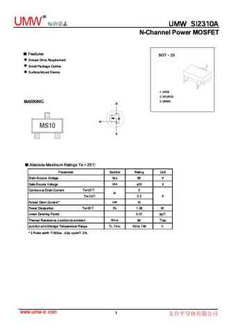
R UMW UMW SI2310A UMW SI2310A UMW SI2310A N-ChanneI Power MOSFET Features SOT 23 Simple Drive Requirement Small Package Outline Surface Mount Device 1. GATE 2. SOURCE 3. DRAIN MARKING D G MS10 S Absolute Maximum Ratings Ta = 25 Parameter Symbol Rating Unit Drain-Source Voltage VD S 60 V GS Gate-Source Voltage V 20 V A Continuous Drain Current ... See More ⇒
si2312a.pdf
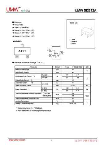
R UMW UMW SI2312A UMW SI2312A Features SOT 23 VDS (V) = 20V ID = 4.9 A (VGS =4.5V) RDS(ON) 33m (VGS = 4.5V) RDS(ON) 40m (VGS = 2.5V) RDS(ON) 51m (VGS = 1.8V) 1. GATE MARKING 2. SOURCE 3. DRAIN G 1 A12T 3 D S 2 Absolute Maximum Ratings Ta = 25 Parameter Symbol 5 sec Steady State Unit Drain-Source Voltage VDS 20 V Gate... See More ⇒
si2319.pdf
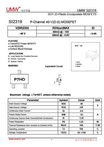
R UMW UMW SI2319 SOT-23 Plastic-Encapsulate MOSFETS SI2319 P-Channel 40-V(D-S) MOSEFET V(BR)DSS RDS(on)MAX ID 45m @ - 10V - 40 V - 4.4A 65m @ - 4.5V FEATURE TrenchFET Power MOSFET SOT 23 Low RDS(ON) Surface Mount Package APPLICATION Load Switch for Portable Devices DC/DC Converter Battery Switch 1. GATE 2. SOURCE MARKING 3. DRAIN Equiva... See More ⇒
si2310.pdf
SI2310 MOSFET ROHS N-Channel Enhancement-Mode MOSFET SOT-23 - Features Advanced trench process technology High Density Cell Design For Ultra Low On-Resistance High Power and Current handing capability MAXIMUM RANTINGS Parameter Symbol Ratings Unit Drain-Source Voltage VDSS 60 V Gate-Source Voltage VGSS 16 Drain Current (Note 1) ID 3.8 A Power Dissipation (N... See More ⇒
si2310.pdf
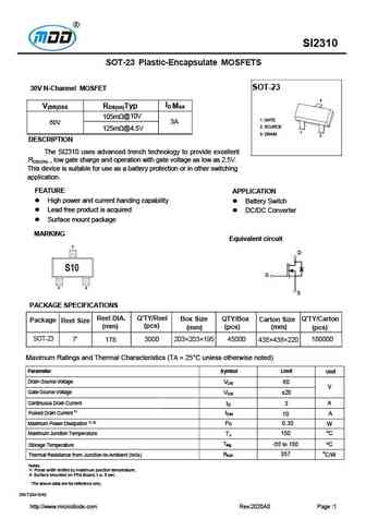
SI2310 SOT-23 Plastic-Encapsulate MOSFETS SOT-23 30V N-Channel MOSFET 3 ID Max V(BR)DSS RDS(on)Typ 105m @10V 1. GATE 3A 60V 2. SOURCE 125m @4.5V 1 3. DRAIN 2 DESCRIPTION The SI2310 uses advanced trench technology to provide excellent RDS(ON) , low gate charge and operation with gate voltage as low as 2.5V. This device is suitable for use as a battery prote... See More ⇒
si2312.pdf
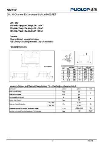
SI2312 20V N-Channel Enhancement Mode MOSFET VDS= 20V RDS(ON), Vgs@4.5V, Ids@5.0A ... See More ⇒
si2310.pdf
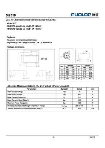
SI2310 20V N-Channel Enhancement Mode MOSFET VDS= 20V RDS(ON), Vgs@4.5V, Ids@5.0A ... See More ⇒
si2312cds-t1-ge3.pdf
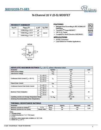
SI2312CDS-T1-GE3 www.VBsemi.tw N-Channel 20 V (D-S) MOSFET FEATURES PRODUCT SUMMARY Halogen-free According to IEC 61249-2-21 VDS (V) RDS(on) ( ) ID (A)e Qg (Typ.) Definition 0.028 at VGS = 4.5 V TrenchFET Power MOSFET 6a 100 % Rg Tested 20 0.042 at VGS = 2.5 V 6a 8.8 nC Compliant to RoHS Directive 2002/95/EC 0.050 at VGS = 1.8 V 5.6 APPLICATIONS DC/... See More ⇒
si2312bds-t1.pdf
SI2312BDS-T1 www.VBsemi.tw N-Channel 20 V (D-S) MOSFET FEATURES PRODUCT SUMMARY Halogen-free According to IEC 61249-2-21 VDS (V) RDS(on) ( ) ID (A)e Qg (Typ.) Definition 0.028 at VGS = 4.5 V TrenchFET Power MOSFET 6a 100 % Rg Tested 20 0.042 at VGS = 2.5 V 6a 8.8 nC Compliant to RoHS Directive 2002/95/EC 0.050 at VGS = 1.8 V 5.6 APPLICATIONS DC/DC C... See More ⇒
si2310.pdf
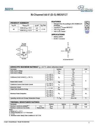
SI2310 www.VBsemi.tw N-Channel 60-V (D-S) MOSFET FEATURES PRODUCT SUMMARY Halogen-free According to IEC 61249-2-21 VDS (V) RDS(on) ( ) ID (A)a Qg (Typ.) Available TrenchFET Power MOSFET 0.085 at VGS = 10 V 4.0 60 2.1 nC 100 % Rg Tested 0.096 at VGS = 4.5 V 3.8 100 % UIS Tested APPLICATIONS Battery Switch DC/DC Converter D TO-236 (SOT23) G 1 ... See More ⇒
si2318ds-t1-ge3.pdf
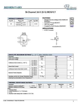
SI2318DS-T1-GE3 www.VBsemi.tw N-Channel 30-V (D-S) MOSFET FEATURES PRODUCT SUMMARY Halogen-free According to IEC 61249-2-21 VDS (V) RDS(on) ( ) ID (A)a Qg (Typ.) Definition 0.030 at VGS = 10 V TrenchFET Power MOSFET 6.5 30 4.5 nC 100 % Rg Tested 0.033 at VGS = 4.5 V 6.0 Compliant to RoHS Directive 2002/95/EC APPLICATIONS DC/DC Converter D TO-236 (SOT... See More ⇒
si2314eds.pdf
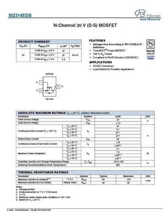
SI2314EDS www.VBsemi.tw N-Channel 20 V (D-S) MOSFET FEATURES PRODUCT SUMMARY Halogen-free According to IEC 61249-2-21 VDS (V) RDS(on) ( ) ID (A)e Qg (Typ.) Definition 0.028 at VGS = 4.5 V TrenchFET Power MOSFET 6a 100 % Rg Tested 20 0.042 at VGS = 2.5 V 6a 8.8 nC Compliant to RoHS Directive 2002/95/EC 0.050 at VGS = 1.8 V 5.6 APPLICATIONS DC/DC Conv... See More ⇒
si2319cds-t1-ge3.pdf

SI2319CDS-T1-GE3 www.VBsemi.tw P-Channel 30 V (D-S) MOSFET FEATURES PRODUCT SUMMARY TrenchFET Power MOSFET 100 % Rg Tested VDS (V) RDS(on) ( ) Typ. ID (A)a Qg (Typ.) 0.046 at VGS = - 10 V - 5.6 0.049 at VGS = - 6 V - 5 11.4 nC - 30 APPLICATIONS 0.054 at VGS = - 4.5 V -4.5 For Mobile Computing - Load Switch - Notebook Adaptor Switch S TO-236 - DC/DC Converter ... See More ⇒
si2319ds-t1-ge3.pdf
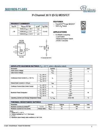
SI2319DS-T1-GE3 www.VBsemi.tw P-Channel 30 V (D-S) MOSFET FEATURES PRODUCT SUMMARY TrenchFET Power MOSFET 100 % Rg Tested VDS (V) RDS(on) ( ) Typ. ID (A)a Qg (Typ.) 0.046 at VGS = - 10 V - 5.6 0.049 at VGS = - 6 V - 5 11.4 nC - 30 APPLICATIONS 0.054 at VGS = - 4.5 V -4.5 For Mobile Computing - Load Switch - Notebook Adaptor Switch S TO-236 - DC/DC Converter ... See More ⇒
si2318cds-t1-ge3.pdf

SI2318CDS-T1-GE3 www.VBsemi.tw N-Channel 30-V (D-S) MOSFET FEATURES PRODUCT SUMMARY Halogen-free According to IEC 61249-2-21 VDS (V) RDS(on) ( ) ID (A)a Qg (Typ.) Definition 0.030 at VGS = 10 V TrenchFET Power MOSFET 6.5 30 4.5 nC 100 % Rg Tested 0.033 at VGS = 4.5 V 6.0 Compliant to RoHS Directive 2002/95/EC APPLICATIONS DC/DC Converter D TO-236 (SO... See More ⇒
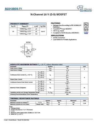
si2312ds.pdf
SI2312DS www.VBsemi.tw N-Channel 20 V (D-S) MOSFET FEATURES PRODUCT SUMMARY Halogen-free According to IEC 61249-2-21 VDS (V) RDS(on) ( ) ID (A)e Qg (Typ.) Definition 0.028 at VGS = 4.5 V TrenchFET Power MOSFET 6a 100 % Rg Tested 20 0.042 at VGS = 2.5 V 6a 8.8 nC Compliant to RoHS Directive 2002/95/EC 0.050 at VGS = 1.8 V 5.6 APPLICATIONS DC/DC Conve... See More ⇒
si2315bds.pdf
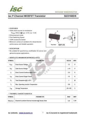
isc P-Channel MOSFET Transistor Si2315BDS FEATURES Static drain-source on-resistance R 52m @V = -4.5V; I = -3.8A DS(on) GS D Enhancement mode Fast Switching Speed 100% avalanche tested Minimum Lot-to-Lot variations for robust device performance and reliable operation DESCRITION Be suitable for synchronous rectification for server and general purpose applications... See More ⇒
Detailed specifications: SI2306BDS, SI2307CDS, SI2308BDS, SI2309CDS, SI2311DS, SI2312BDS, SI2312CDS, SI2316BDS, IRFZ24N, SI2319CDS, SI2321, SI2323CDS, SI2323DDS, SI2327DS, SI2329DS, SI2331DS, SI2333DDS
Keywords - SI2316DS MOSFET specs
SI2316DS cross reference
SI2316DS equivalent finder
SI2316DS pdf lookup
SI2316DS substitution
SI2316DS replacement
Need a MOSFET replacement? Our guide shows you how to find a perfect substitute by comparing key parameters and specs
History: FQD2N100 | 2SJ0398 | FR2307Z | BRD7N65S
🌐 : EN ES РУ

LIST
Last Update
MOSFET: AUB062N08BG | AUB060N08AG | AUB056N10 | AUB056N08BGL | AUB050N085 | AUB050N055 | AUB045N12 | AUB045N10BT | AUB039N10 | AUB034N10
Popular searches
2n3405 | 2n3567 | 2sc1226 | 2sd180 | 2sd235 | k3502 datasheet | p0903bdg datasheet | 2sa722