SI3442BDV Specs and Replacement
Type Designator: SI3442BDV
Type of Transistor: MOSFET
Type of Control Channel: N-Channel
Absolute Maximum Ratings
Pd ⓘ - Maximum Power Dissipation: 0.86 W
|Vds|ⓘ - Maximum Drain-Source Voltage: 20 V
|Vgs|ⓘ - Maximum Gate-Source Voltage: 12 V
|Id| ⓘ - Maximum Drain Current: 3 A
Tj ⓘ - Maximum Junction Temperature: 150 °C
Electrical Characteristics
tr ⓘ - Rise Time: 50 nS
Cossⓘ - Output Capacitance: 75 pF
RDSonⓘ - Maximum Drain-Source On-State Resistance: 0.057 Ohm
Package: TSOP-6
SI3442BDV substitution
- MOSFET ⓘ Cross-Reference Search
SI3442BDV datasheet
si3442bdv.pdf
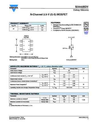
Si3442BDV Vishay Siliconix N-Channel 2.5-V (G-S) MOSFET FEATURES PRODUCT SUMMARY Halogen-free According to IEC 61249-2-21 VDS (V) RDS(on) ( )ID (A) Definition 0.057 at VGS = 4.5 V 4.2 TrenchFET Power MOSFET 20 0.090 at VGS = 2.5 V 3.4 Compliant to RoHS Directive 2002/95/EC TSOP-6 (1, 2, 5, 6) D Top View 1 6 3 mm 5 2 (3) G 3 4 2.85 mm (4) S Ordering... See More ⇒
si3442bd.pdf

Si3442BDV Vishay Siliconix N-Channel 2.5-V (G-S) MOSFET FEATURES PRODUCT SUMMARY Halogen-free According to IEC 61249-2-21 VDS (V) RDS(on) ( )ID (A) Definition 0.057 at VGS = 4.5 V 4.2 TrenchFET Power MOSFET 20 0.090 at VGS = 2.5 V 3.4 Compliant to RoHS Directive 2002/95/EC TSOP-6 (1, 2, 5, 6) D Top View 1 6 3 mm 5 2 (3) G 3 4 2.85 mm (4) S Ordering... See More ⇒
si3442cdv.pdf
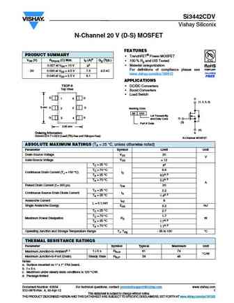
Si3442CDV Vishay Siliconix N-Channel 20 V (D-S) MOSFET FEATURES PRODUCT SUMMARY TrenchFET Power MOSFET VDS (V) RDS(on) ( ) Max. ID (A)a Qg (Typ.) 100 % Rg and UIS Tested Material categorization 0.027 at VGS = 10 V 8d For definitions of compliance please see 20 0.030 at VGS = 4.5 V 7.5 4.3 nC www.vishay.com/doc?99912 0.049 at VGS = 2.5 V 6.1 APPLICATIONS TSO... See More ⇒
si3442dv.pdf
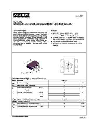
March 2001 SI3442DV N-Channel Logic Level Enhancement Mode Field Effect Transistor General Description Features These N-Channel logic level enhancement mode power field 4.1 A, 20 V. RDS(ON) = 0.06 @ VGS = 4.5 V effect transistors are produced using Fairchild's proprietary, RDS(ON) = 0.075 @ VGS =2.7 V. high cell density, DMOS technology. This very high density process is tai... See More ⇒
Detailed specifications: SI3429EDV, SI3430DV, SI3433CDV, SI3434, SI3434DV, SI3438DV, SI3440DV, SI3441BDV, AO3400, SI3442CDV, SI3442DV, SI3443BDV, SI3443CDV, SI3443DDV, SI3443DVTR, SI3445ADV, SI3445DV
Keywords - SI3442BDV MOSFET specs
SI3442BDV cross reference
SI3442BDV equivalent finder
SI3442BDV pdf lookup
SI3442BDV substitution
SI3442BDV replacement
Learn how to find the right MOSFET substitute. A guide to cross-reference, check specs and replace MOSFETs in your circuits.
🌐 : EN ES РУ

LIST
Last Update
MOSFET: AUB062N08BG | AUB060N08AG | AUB056N10 | AUB056N08BGL | AUB050N085 | AUB050N055 | AUB045N12 | AUB045N10BT | AUB039N10 | AUB034N10
Popular searches
2sa1011 | 2sa1283 | 2sb646 | 2sc1885 datasheet | 2sc2580 | 2sc710 | 2sc968 | 2sd217