IRFS630A Specs and Replacement
Type Designator: IRFS630A
Type of Transistor: MOSFET
Type of Control Channel: N-Channel
Absolute Maximum Ratings
Pd ⓘ - Maximum Power Dissipation: 38 W
|Vds|ⓘ - Maximum Drain-Source Voltage: 200 V
|Vgs|ⓘ - Maximum Gate-Source Voltage: 30 V
|Id| ⓘ - Maximum Drain Current: 6.5 A
Tj ⓘ - Maximum Junction Temperature: 150 °C
Electrical Characteristics
tr ⓘ - Rise Time: 13 nS
Cossⓘ - Output Capacitance: 95 pF
RDSonⓘ - Maximum Drain-Source On-State Resistance: 0.4 Ohm
Package: TO220F
IRFS630A substitution
- MOSFET ⓘ Cross-Reference Search
IRFS630A datasheet
irfs630a.pdf

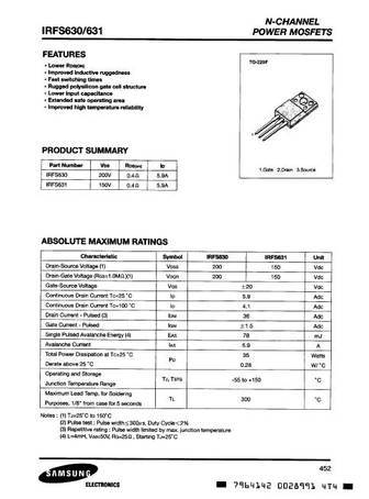
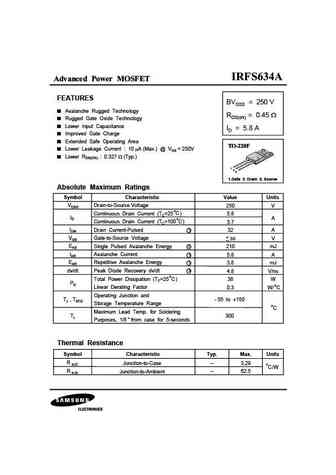
Advanced Power MOSFET FEATURES BVDSS = 200 V Avalanche Rugged Technology RDS(on) = 0.4 Rugged Gate Oxide Technology Lower Input Capacitance ID = 6.5 A Improved Gate Charge Extended Safe Operating Area Lower Leakage Current 10 A (Max.) @ VDS = 200V Low RDS(ON) 0.333 (Typ.) 1 2 3 1.Gate 2. Drain 3. Source Absolute Maximum Ratings Symbol Characteristic Valu... See More ⇒
irf630b irfs630b.pdf
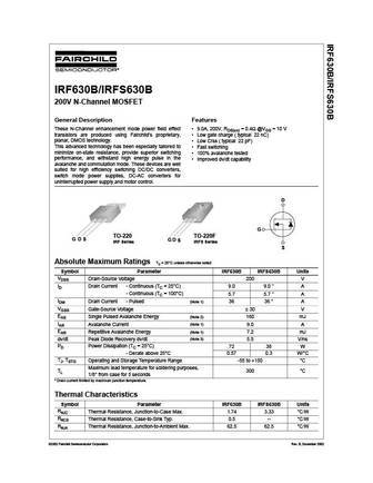
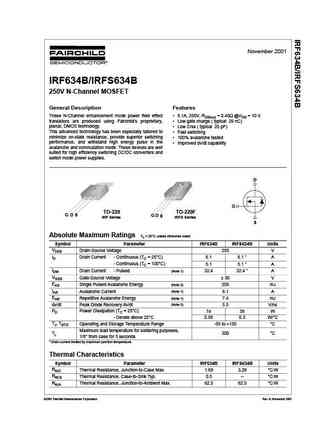
IRF630B/IRFS630B 200V N-Channel MOSFET General Description Features These N-Channel enhancement mode power field effect 9.0A, 200V, RDS(on) = 0.4 @VGS = 10 V transistors are produced using Fairchild s proprietary, Low gate charge ( typical 22 nC) planar, DMOS technology. Low Crss ( typical 22 pF) This advanced technology has been especially tailored to Fast switchin... See More ⇒
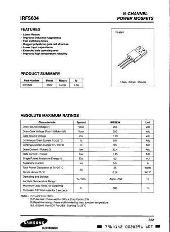
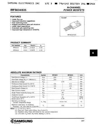

Detailed specifications: IRFS614A, IRFS620, IRFS620A, IRFS622, IRFS624, IRFS624A, IRFS625, IRFS630, IRF530, IRFS632, IRFS634, IRFS634A, IRFS635, IRFS640, IRFS640A, IRFS642, IRFS644
Keywords - IRFS630A MOSFET specs
IRFS630A cross reference
IRFS630A equivalent finder
IRFS630A pdf lookup
IRFS630A substitution
IRFS630A replacement
Can't find your MOSFET? Learn how to find a substitute transistor by analyzing voltage, current and package compatibility
History: FDB14N30 | J309G
🌐 : EN ES РУ

LIST
Last Update
MOSFET: ASU70R600E | ASU65R850E | ASU65R550E | ASU65R350E | ASR65R120EFD | ASR65R046EFD | ASQ65R046EFD | ASM65R280E | ASM60R330E | ASE70R950E
Popular searches
2sa992 | 2sa970 | a970 | d2390 transistor | 2n5087 equivalent | tip147 datasheet | 2n4124 | mj15022