SSF2418B Datasheet. Specs and Replacement
Type Designator: SSF2418B 📄📄
Type of Transistor: MOSFET
Type of Control Channel: N-Channel
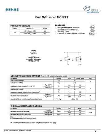
Absolute Maximum Ratings
Pd ⓘ - Maximum Power Dissipation: 1.3 W
|Vds|ⓘ - Maximum Drain-Source Voltage: 20 V
|Vgs|ⓘ - Maximum Gate-Source Voltage: 12 V
|Id| ⓘ - Maximum Drain Current: 6 A
Tj ⓘ - Maximum Junction Temperature: 150 °C
Electrical Characteristics
tr ⓘ - Rise Time: 50 nS
Cossⓘ - Output Capacitance: 170 pF
RDSonⓘ - Maximum Drain-Source On-State Resistance: 0.021 Ohm
Package: SOT-23-6
SSF2418B substitution
- MOSFET ⓘ Cross-Reference Search
SSF2418B datasheet
ssf2418b.pdf
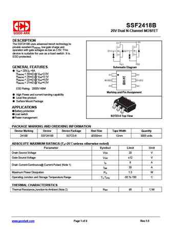
SSF2418B 20V Dual N-Channel MOSFET DESCRIPTION The SSF2418B uses advanced trench technology to provide excellent RDS(ON), low gate charge and operation with gate voltages as low as 2.5V. This device is suitable for use as a load switch. It is ESD protected. Schematic Diagram GENERAL FEATURES VDS = 20V,ID =6A RDS(ON) ... See More ⇒
ssf2418eb.pdf
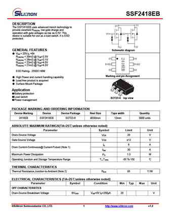
SSF2418EB DESCRIPTION The SSF2418EB uses advanced trench technology to provide excellent RDS(ON), low gate charge and operation with gate voltages as low as 0.5V. This device is suitable for use as a load switch. It is ESD protected. Schematic diagram GENERAL FEATURES VDS = 20V,ID =6A RDS(ON) ... See More ⇒
ssf2418e.pdf
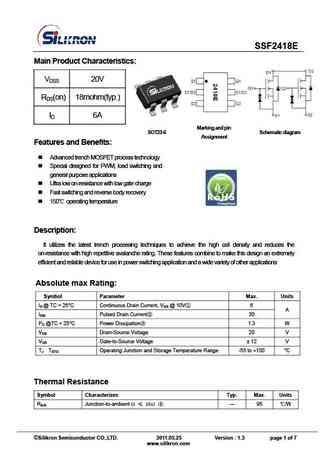
SSF2418E Main Product Characteristics VDSS 20V RDS(on) 18mohm(typ.) ID 6A Mark ing an d pi n SOT23-6 Schema t ic diagr a m Assignment Features and Benefits Advanced trench MOSFET process technology Special designed for PWM, load switching and general purpose applications Ultra low on-resistance with low gate charge Fast switching and reverse body re... See More ⇒
ssf2418ebk.pdf
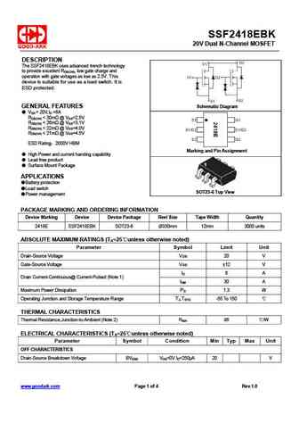
SSF2418EBK 20V Dual N-Channel MOSFET DESCRIPTION The SSF2418EBK uses advanced trench technology to provide excellent RDS(ON), low gate charge and operation with gate voltages as low as 2.5V. This device is suitable for use as a load switch. It is ESD protected. Schematic Diagram GENERAL FEATURES VDS = 20V,ID =6A RDS(ON) ... See More ⇒
Detailed specifications: SQP50P03-07, SQP60N06-15, SQP90P06-07L, SQR40N10-25, SQR50N03-06P, SQR50N04-3M8, SQR50N06-07L, SSF22A5E, IRF2807, SSF2418EBK, SSF2439E, SSF2641S, SSF2816EBK, SSF2N60D1, SSF3612E, R9523, SSF440M
Keywords - SSF2418B MOSFET specs
SSF2418B cross reference
SSF2418B equivalent finder
SSF2418B pdf lookup
SSF2418B substitution
SSF2418B replacement
Step-by-step guide to finding a MOSFET replacement. Cross-reference parts and ensure compatibility for your repair or project.
History: HGN210N12SL | HGN200N10SL
🌐 : EN ES РУ

LIST
Last Update
MOSFET: ASDM30P100KQ | ASDM30N90Q | ASDM30N75KQ | ASDM30N150Q | ASDM30N120Q | ASDM30N120KQ | ASDM30N100KQ | ASDM30DN40E | ASDM30DN30E | ASDM3050KQ
Popular searches
75n65kdf | c2274 transistor | c5200 2sc5200 transistor datasheet | d2390 datasheet | 2sa750 replacement | 2sc984 replacement | a1046 transistor | hy19p03