TK20A60W Datasheet. Specs and Replacement
Type Designator: TK20A60W 📄📄
Type of Transistor: MOSFET
Type of Control Channel: N-Channel
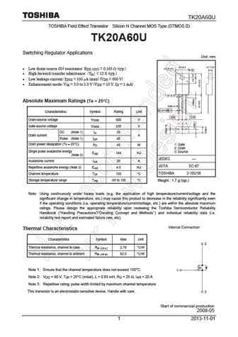
Absolute Maximum Ratings
Pd ⓘ - Maximum Power Dissipation: 45 W
|Vds|ⓘ - Maximum Drain-Source Voltage: 600 V
|Vgs|ⓘ - Maximum Gate-Source Voltage: 30 V
|Id| ⓘ - Maximum Drain Current: 20 A
Tj ⓘ - Maximum Junction Temperature: 150 °C
Electrical Characteristics
tr ⓘ - Rise Time: 25 nS
Cossⓘ - Output Capacitance: 40 pF
RDSonⓘ - Maximum Drain-Source On-State Resistance: 0.155 Ohm
Package: TO-220SIS
📄📄 Copy
TK20A60W substitution
- MOSFET ⓘ Cross-Reference Search
TK20A60W datasheet
tk20a60w.pdf
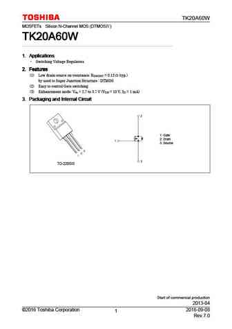
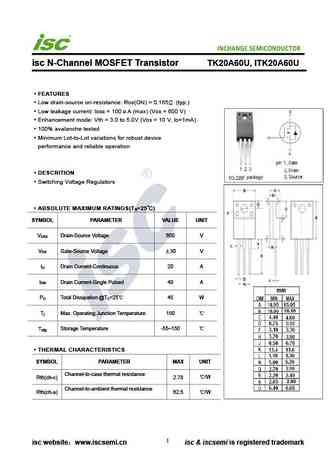
TK20A60W MOSFETs Silicon N-Channel MOS (DTMOS ) TK20A60W TK20A60W TK20A60W TK20A60W 1. Applications 1. Applications 1. Applications 1. Applications Switching Voltage Regulators 2. Features 2. Features 2. Features 2. Features (1) Low drain-source on-resistance RDS(ON) = 0.13 (typ.) by used to Super Junction Structure DTMOS (2) Easy to control Gate switching (3) En... See More ⇒
tk20a60w.pdf
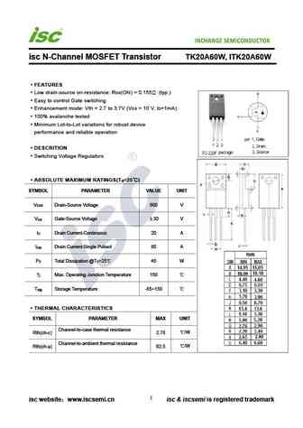
INCHANGE Semiconductor isc N-Channel MOSFET Transistor TK20A60W, ITK20A60W FEATURES Low drain-source on-resistance RDS(ON) = 0.155 (typ.) Easy to control Gate switching Enhancement mode Vth = 2.7 to 3.7V (VDS = 10 V, ID=1mA) 100% avalanche tested Minimum Lot-to-Lot variations for robust device performance and reliable operation DESCRITION Switching Voltage Regulat... See More ⇒
tk20a60w5.pdf
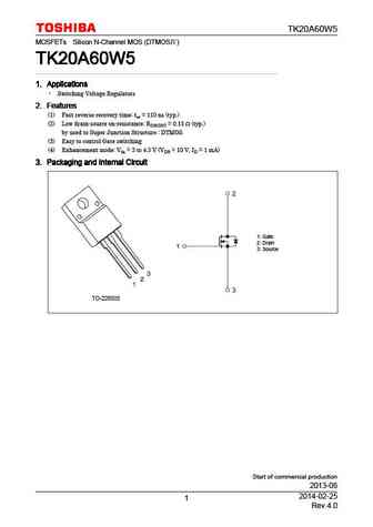
TK20A60W5 MOSFETs Silicon N-Channel MOS (DTMOS ) TK20A60W5 TK20A60W5 TK20A60W5 TK20A60W5 1. Applications 1. Applications 1. Applications 1. Applications Switching Voltage Regulators 2. Features 2. Features 2. Features 2. Features (1) Fast reverse recovery time trr = 110 ns (typ.) (2) Low drain-source on-resistance RDS(ON) = 0.15 (typ.) by used to Super Junction Str... See More ⇒
tk20a60w5.pdf
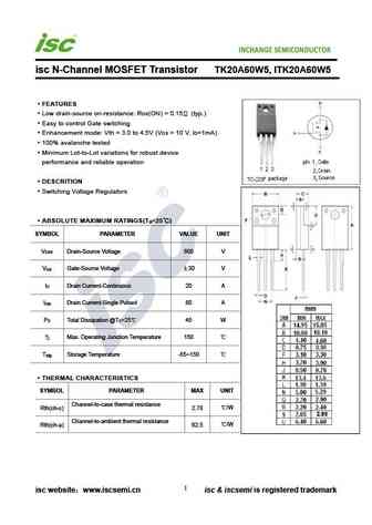
INCHANGE Semiconductor isc N-Channel MOSFET Transistor TK20A60W5, ITK20A60W5 FEATURES Low drain-source on-resistance RDS(ON) = 0.15 (typ.) Easy to control Gate switching Enhancement mode Vth = 3.0 to 4.5V (VDS = 10 V, ID=1mA) 100% avalanche tested Minimum Lot-to-Lot variations for robust device performance and reliable operation DESCRITION Switching Voltage Regula... See More ⇒
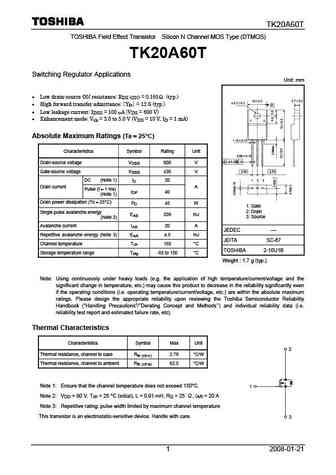
Detailed specifications: TK16V60W5, TK17A80W, TK17C65W, TK17E65W, TK17N65W, TK17V65W, TK18E10K3, TK200F04N1L, RFP50N06, TK20A60W5, TK20C60W, TK20E60W, TK20E60W5, TK20G60W, TK20J60W, TK20J60W5, TK20N60W
Keywords - TK20A60W MOSFET specs
TK20A60W cross reference
TK20A60W equivalent finder
TK20A60W pdf lookup
TK20A60W substitution
TK20A60W replacement
Need a MOSFET replacement? Our guide shows you how to find a perfect substitute by comparing key parameters and specs
MOSFET Parameters. How They Affect Each Other
History: CEM3109 | APTM100A13SCG | CTP10P095 | CS50N06 | QM03N65D | BUK9618-30 | HM80N03A
🌐 : EN ES РУ

LIST
Last Update
MOSFET: CS95118 | CS85105A | CS75N45 | CS72N12 | CS55N50 | CS48N75A | CS40N27 | MSQ60P04D | MSQ40P07D | MSQ30P40D
Popular searches
irf840 | irf740 | c945 transistor | irf640n | 2n3904 | bc547 datasheet | k3797 mosfet | bs170 datasheet