TK6A65W Specs and Replacement
Type Designator: TK6A65W
Type of Transistor: MOSFET
Type of Control Channel: N-Channel
Absolute Maximum Ratings
Pd ⓘ - Maximum Power Dissipation: 30 W
|Vds|ⓘ - Maximum Drain-Source Voltage: 650 V
|Vgs|ⓘ - Maximum Gate-Source Voltage: 30 V
|Id| ⓘ - Maximum Drain Current: 5.8 A
Tj ⓘ - Maximum Junction Temperature: 150 °C
Electrical Characteristics
tr ⓘ - Rise Time: 14 nS
Cossⓘ - Output Capacitance: 12 pF
RDSonⓘ - Maximum Drain-Source On-State Resistance: 1 Ohm
Package: TO-220SIS
TK6A65W substitution
- MOSFET ⓘ Cross-Reference Search
TK6A65W datasheet
tk6a65w.pdf
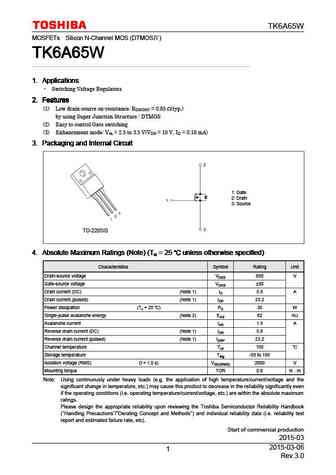
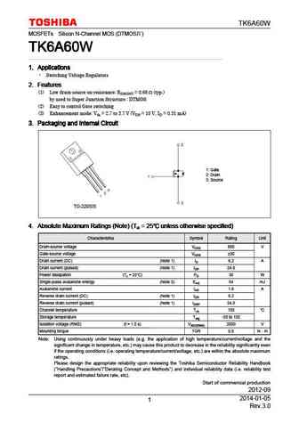
TK6A65W MOSFETs Silicon N-Channel MOS (DTMOS ) TK6A65W TK6A65W TK6A65W TK6A65W 1. Applications 1. Applications 1. Applications 1. Applications Switching Voltage Regulators 2. Features 2. Features 2. Features 2. Features (1) Low drain-source on-resistance RDS(ON) = 0.85 (typ.) by using Super Junction Structure DTMOS (2) Easy to control Gate switching (3) Enhancement... See More ⇒
tk6a65w.pdf
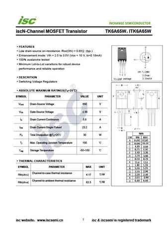
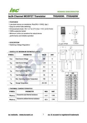
INCHANGE Semiconductor iscN-Channel MOSFET Transistor TK6A65W ITK6A65W FEATURES Low drain-source on-resistance RDS(ON) = 0.85 (typ.) Enhancement mode Vth = 2.5 to 3.5V (VDS = 10 V, ID=0.18mA) 100% avalanche tested Minimum Lot-to-Lot variations for robust device performance and reliable operation DESCRITION Switching Voltage Regulators ABSOLUTE MAXIMUM RATINGS(... See More ⇒
tk6a65d.pdf
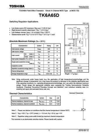
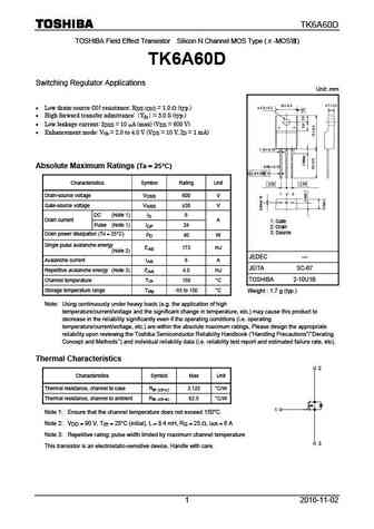
TK6A65D TOSHIBA Field Effect Transistor Silicon N Channel MOS Type ( -MOS VII) TK6A65D Switching Regulator Applications Unit mm Low drain-source ON resistance RDS (ON) = 0.95 (typ.) High forward transfer admittance Yfs = 4.0 S (typ.) Low leakage current IDSS = 10 A (max) (VDS = 650 V) Enhancement-mode Vth = 2.0 to 4.0 V (VDS = 10 V, ID = 1 mA) ... See More ⇒
tk6a65d.pdf
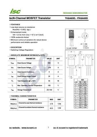
INCHANGE Semiconductor iscN-Channel MOSFET Transistor TK6A65D ITK6A65D FEATURES Low drain-source on-resistance RDS(ON) = 0.95 (typ.) Enhancement mode Vth = 2.0 to 4.0V (VDS = 10 V, ID=1.0mA) 100% avalanche tested Minimum Lot-to-Lot variations for robust device performance and reliable operation DESCRITION Switching Voltage Regulators ABSOLUTE MAXIMUM RATINGS(T... See More ⇒
Detailed specifications: TK62J60W, TK62J60W5, TK62N60W, TK62N60W5, TK62N60X, TK65G10N1, TK65S04N1L, TK6A60W, 12N60, TK6A80E, TK6P60W, TK6P65W, TK6Q60W, TK6Q65W, TK70J04K3Z, TK72A08N1, TK72A12N1
Keywords - TK6A65W MOSFET specs
TK6A65W cross reference
TK6A65W equivalent finder
TK6A65W pdf lookup
TK6A65W substitution
TK6A65W replacement
Need a MOSFET replacement? Our guide shows you how to find a perfect substitute by comparing key parameters and specs
History: 3080K | SM9994DSO | SM6128NSQG | 2SK3299 | TK6P60W | 2SK818 | BSC031N06NS3G
🌐 : EN ES РУ

LIST
Last Update
MOSFET: AUB034N10 | AUB033N08BG | AUB026N085 | AUA062N08BG | AUA060N08AG | AUA056N08BGL | AUA039N10 | ASW80R290E | ASW65R120EFD | ASW65R110E
Popular searches
irf 3205 | 2n5088 equivalent | d882 transistor | 2n3771 | s9018 | 2n3904 equivalent | ksa1220 | s9015