TK7A60W Specs and Replacement
Type Designator: TK7A60W
Type of Transistor: MOSFET
Type of Control Channel: N-Channel
Absolute Maximum Ratings
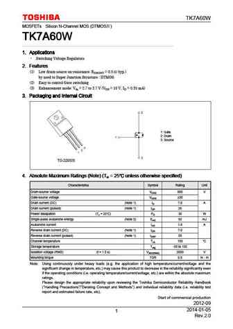
Pd ⓘ - Maximum Power Dissipation: 30 W
|Vds|ⓘ - Maximum Drain-Source Voltage: 600 V
|Vgs|ⓘ - Maximum Gate-Source Voltage: 30 V
|Id| ⓘ - Maximum Drain Current: 7 A
Tj ⓘ - Maximum Junction Temperature: 150 °C
Electrical Characteristics
tr ⓘ - Rise Time: 18 nS
Cossⓘ - Output Capacitance: 13 pF
RDSonⓘ - Maximum Drain-Source On-State Resistance: 0.6 Ohm
Package: TO-220SIS
TK7A60W substitution
- MOSFET ⓘ Cross-Reference Search
TK7A60W datasheet
tk7a60w.pdf
TK7A60W MOSFETs Silicon N-Channel MOS (DTMOS ) TK7A60W TK7A60W TK7A60W TK7A60W 1. Applications 1. Applications 1. Applications 1. Applications Switching Voltage Regulators 2. Features 2. Features 2. Features 2. Features (1) Low drain-source on-resistance RDS(ON) = 0.5 (typ.) by used to Super Junction Structure DTMOS (2) Easy to control Gate switching (3) Enhancem... See More ⇒
tk7a60w.pdf
INCHANGE Semiconductor iscN-Channel MOSFET Transistor TK7A60W ITK7A60W FEATURES Low drain-source on-resistance RDS(ON) = 0.5 (typ.) Easy to control Gate switching Enhancement mode Vth = 2.7 to 3.7V (VDS = 10 V, ID=0.35mA) 100% avalanche tested Minimum Lot-to-Lot variations for robust device performance and reliable operation DESCRITION Switching Voltage Regulato... See More ⇒
tk7a60w5.pdf
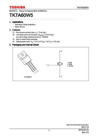
TK7A60W5 MOSFETs Silicon N-Channel MOS (DTMOS ) TK7A60W5 TK7A60W5 TK7A60W5 TK7A60W5 1. Applications 1. Applications 1. Applications 1. Applications Switching Voltage Regulators Motor Drivers 2. Features 2. Features 2. Features 2. Features (1) Fast reverse recovery time trr = 75 ns (typ.) (2) Low drain-source on-resistance RDS(ON) = 0.54 (typ.) by used to Super... See More ⇒
tk7a60w5.pdf
INCHANGE Semiconductor iscN-Channel MOSFET Transistor TK7A60W5 ITK7A60W5 FEATURES Low drain-source on-resistance RDS(ON) = 0.54 (typ.) Easy to control Gate switching Enhancement mode Vth = 3 to 4.5V (VDS = 10 V, ID=0.35mA) 100% avalanche tested Minimum Lot-to-Lot variations for robust device performance and reliable operation DESCRITION Switching Voltage Regulat... See More ⇒
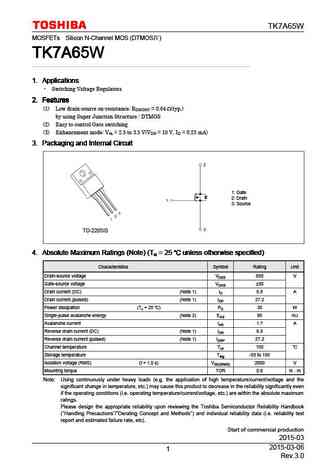
Detailed specifications: TK6P65W, TK6Q60W, TK6Q65W, TK70J04K3Z, TK72A08N1, TK72A12N1, TK72E08N1, TK72E12N1, TK10A60D, TK7A60W5, TK7A65W, TK7A90E, TK7J90E, TK7P60W, TK7P60W5, TK7P65W, TK7Q60W
Keywords - TK7A60W MOSFET specs
TK7A60W cross reference
TK7A60W equivalent finder
TK7A60W pdf lookup
TK7A60W substitution
TK7A60W replacement
Learn how to find the right MOSFET substitute. A guide to cross-reference, check specs and replace MOSFETs in your circuits.
History: 5N70GS
🌐 : EN ES РУ
LIST
Last Update
MOSFET: ASU70R600E | ASU65R850E | ASU65R550E | ASU65R350E | ASR65R120EFD | ASR65R046EFD | ASQ65R046EFD | ASM65R280E | ASM60R330E | ASE70R950E
Popular searches
mj2955 | mje15030 | 2n3904 transistor | 2sd424 | 2sc828 | 2n4125 | tip42c transistor | c1815 transistor datasheet


