TMU5N60Z Datasheet. Specs and Replacement
Type Designator: TMU5N60Z 📄📄
Type of Transistor: MOSFET
Type of Control Channel: N-Channel
Absolute Maximum Ratings
Pd ⓘ - Maximum Power Dissipation: 98.4 W
|Vds|ⓘ - Maximum Drain-Source Voltage: 600 V
|Vgs|ⓘ - Maximum Gate-Source Voltage: 30 V
|Id| ⓘ - Maximum Drain Current: 4.2 A
Tj ⓘ - Maximum Junction Temperature: 150 °C
Electrical Characteristics
tr ⓘ - Rise Time: 27 nS
Cossⓘ - Output Capacitance: 69 pF
RDSonⓘ - Maximum Drain-Source On-State Resistance: 2.1 Ohm
Package: I-PAK
📄📄 Copy
TMU5N60Z substitution
- MOSFET ⓘ Cross-Reference Search
TMU5N60Z datasheet
tmd5n60z tmu5n60z.pdf
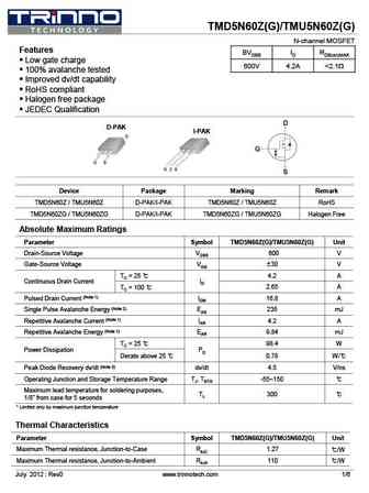
TMD5N60Z(G)/TMU5N60Z(G) N-channel MOSFET Features BVDSS ID RDS(on)MAX Low gate charge 600V 4.2A ... See More ⇒
tmd5n60az tmu5n60az.pdf
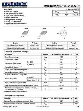
TMD5N60AZ(G)/TMU5N60AZ(G) N-channel MOSFET Features Low gate charge BVDSS ID RDS(on) 100% avalanche tested 600V 4.2A ... See More ⇒
tmd5n50 tmd5n50g tmu5n50 tmu5n50g.pdf
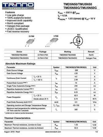
TMD5N50/TMU5N50 TMD5N50G/TMU5N50G Features VDSS = 550 V @Tjmax Low gate charge ID = 4.5A 100% avalanche tested RDS(ON) = 1.65 W(max) @ VGS= 10 V Improved dv/dt capability RoHS compliant Halogen free package JEDEC Qualification Fast reverse recovery D I-PAK D-PAK G S Device Package Marking Remark TMD5N50/TMU5N50 D-PAK/I-PAK TMD5N50/TMU5N50 RoHS ... See More ⇒
tmd5n40zg tmu5n40zg.pdf
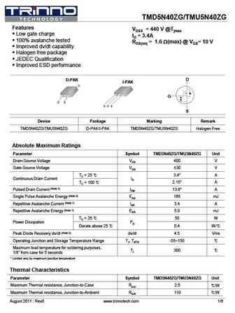
TMD5N40ZG/TMU5N40ZG Features VDSS = 440 V @Tjmax Low gate charge ID = 3.4A 100% avalanche tested RDS(on) = 1.6 W(max) @ VGS= 10 V Improved dv/dt capability Halogen free package JEDEC Qualification Improved ESD performance D-PAK D I-PAK G S Device Package Marking Remark TMD5N40ZG/TMU5N40ZG D-PAK/I-PAK TMD5N40ZG/TMU5N40ZG Halogen Free Abso... See More ⇒
Detailed specifications: TMU4N60, TMU4N60AZ, TMU4N65AZ, TMU4N65Z, TMU5N40ZG, TMU5N50, TMU5N50G, TMU5N60AZ, STF13NM60N, TMU630Z, TMU6N65G, TMU7N60Z, TMU7N65AZ, TMU7N65Z, TMU830, TMU830AZ, TMU830Z
Keywords - TMU5N60Z MOSFET specs
TMU5N60Z cross reference
TMU5N60Z equivalent finder
TMU5N60Z pdf lookup
TMU5N60Z substitution
TMU5N60Z replacement
Can't find your MOSFET? Learn how to find a substitute transistor by analyzing voltage, current and package compatibility
MOSFET Parameters. How They Affect Each Other
History: TMD7N60Z
🌐 : EN ES РУ

LIST
Last Update
MOSFET: BC3134KT | BC3134K | BC2302W | BC2302T-2.8A | BC2302-2.8A | BC2301W | BC2301T-2.8A | CB3139KTB | CB2301DW | BC8205
Popular searches
2n1304 | 2sa979 | 2sc4793 | d965 | mje15031 | irfp150n | mj15025 | mp1620