TMU6N65G Specs and Replacement
Type Designator: TMU6N65G
Type of Transistor: MOSFET
Type of Control Channel: N-Channel
Absolute Maximum Ratings
Pd ⓘ - Maximum Power Dissipation: 120 W
|Vds|ⓘ - Maximum Drain-Source Voltage: 650 V
|Vgs|ⓘ - Maximum Gate-Source Voltage: 30 V
|Id| ⓘ - Maximum Drain Current: 5.5 A
Tj ⓘ - Maximum Junction Temperature: 150 °C
Electrical Characteristics
tr ⓘ - Rise Time: 30 nS
Cossⓘ - Output Capacitance: 90 pF
RDSonⓘ - Maximum Drain-Source On-State Resistance: 1.6 Ohm
Package: I-PAK
TMU6N65G substitution
- MOSFET ⓘ Cross-Reference Search
TMU6N65G datasheet
tmd6n65g tmu6n65g.pdf
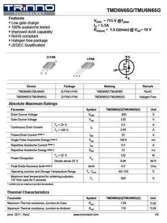
TMD6N65G/TMU6N65G Features VDSS = 715 V @Tjmax Low gate charge ID = 5.5A 100% avalanche tested RDS(on) = 1.6 W(max) @ VGS= 10 V Improved dv/dt capability RoHS compliant Halogen free package JEDEC Qualification D-PAK D I-PAK G S Device Package Marking Remark TMD6N65/TMU6N65 D-PAK/I-PAK TMD6N65/TMU6N65 RoHS TMD6N65G/TMU6N65G D-PAK/I-PAK TM... See More ⇒
tmd6n70g tmu6n70g tmd6n70 tmu6n70.pdf
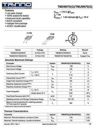
TMD6N70(G)/TMU6N70(G) Features VDSS = 770 V @Tjmax Low gate charge ID = 5A 100% avalanche tested RDS(on) = 1.65 W(max) @ VGS= 10 V Improved dv/dt capability RoHS compliant Halogen free package JEDEC Qualification D-PAK D I-PAK G S Device Package Marking Remark TMD6N70/TMU6N70 D-PAK/I-PAK TMD6N70/TMU6N70 RoHS TMD6N70G/TMU6N70G D-PAK/I-PAK... See More ⇒
Detailed specifications: TMU4N65AZ, TMU4N65Z, TMU5N40ZG, TMU5N50, TMU5N50G, TMU5N60AZ, TMU5N60Z, TMU630Z, 18N50, TMU7N60Z, TMU7N65AZ, TMU7N65Z, TMU830, TMU830AZ, TMU830Z, TMU8N25Z, TMU8N50Z
Keywords - TMU6N65G MOSFET specs
TMU6N65G cross reference
TMU6N65G equivalent finder
TMU6N65G pdf lookup
TMU6N65G substitution
TMU6N65G replacement
Learn how to find the right MOSFET substitute. A guide to cross-reference, check specs and replace MOSFETs in your circuits.
