SD214DE Specs and Replacement
Type Designator: SD214DE
Type of Transistor: MOSFET
Type of Control Channel: N-Channel
Absolute Maximum Ratings
Pd ⓘ
- Maximum Power Dissipation: 1.2 W
|Vds|ⓘ - Maximum Drain-Source Voltage: 20 V
|Vgs|ⓘ - Maximum Gate-Source Voltage: 40 V
|Id| ⓘ - Maximum Drain Current: 0.05 A
Tj ⓘ - Maximum Junction Temperature: 125 °C
Electrical Characteristics
Rds ⓘ - Maximum Drain-Source On-State Resistance: 45 Ohm
Package: TO-72
- MOSFET ⓘ Cross-Reference Search
SD214DE datasheet
..1. Size:29K calogic
sd210de sd212de sd214de.pdf 
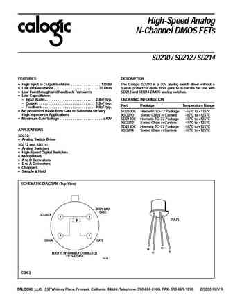
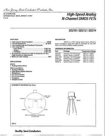
High-Speed Analog N-Channel DMOS FETs SD210 / SD212 / SD214 FEATURES DESCRIPTION High Input to Output Isolation . . . . . . . . . . . . . . . . 120dB The Calogic SD210 is a 30V analog switch driver without a Low On Resistance . . . . . . . . . . . . . . . . . . . . . . . . 30 Ohm built-in protection diode from gate to substrate for use with Low Feedthrough and Feedba... See More ⇒
9.2. Size:48K rohm
2sd2142.pdf
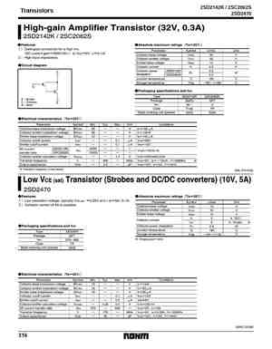
2SD2142K / 2SC2062S Transistors Transistors 2SD2470 (94L-570-D25) (SPEC-D230) 316 Appendix Notes No technical content pages of this document may be reproduced in any form or transmitted by any means without prior permission of ROHM CO.,LTD. The contents described herein are subject to change without notice. The specifications for the product described in this document are for ref... See More ⇒
9.3. Size:87K rohm
2sd2212 2sd2143 2sd1866.pdf
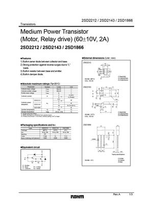
2SD2212 / 2SD2143 / 2SD1866 Transistors Medium Power Transistor (Motor, Relay drive) (60 10V, 2A) 2SD2212 / 2SD2143 / 2SD1866 External dimensions (Unit mm) Features 1) Built-in zener diode between collector and base. 2SD2212 4.0 2) Strong protection against reverse surges due to "L" 1.0 2.5 0.5 loads. (1) (2) 3) Built-in resistor between base and emitter. (3) 4) ... See More ⇒
9.4. Size:53K rohm
2sd2144s.pdf
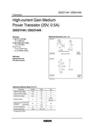
2SD2114K / 2SD2144S Transistors High-current Gain Medium Power Transistor (20V, 0.5A) 2SD2114K / 2SD2144S External dimensions (Units mm) Features 2SD2114K 1) High DC current gain. 2.9 0.2 1.1+0.2 1.9 0.2 -0.1 hFE = 1200 (Typ.) 0.8 0.1 0.95 0.95 2) High emitter-base voltage. (1) (2) 0 0.1 VEBO =12V (Min.) 3) Low VCE (sat). (3) VCE (sat) = 0.18V (Typ.) +0.1 0.15... See More ⇒
9.5. Size:89K rohm
2sd2114k 2sd2144s.pdf

2SD2114K / 2SD2144S Transistors High-current Gain Medium Power Transistor (20V, 0.5A) 2SD2114K / 2SD2144S External dimensions (Unit mm) Features 1) High DC current gain. 2SD2114K 2.9 0.2 1.1+0.2 1.9 0.2 -0.1 hFE = 1200 (Typ.) 0.8 0.1 0.95 0.95 2) High emitter-base voltage. (1) (2) 0 0.1 VEBO =12V (Min.) 3) Low VCE (sat). (3) +0.1 VCE (sat) = 0.18V (Ty... See More ⇒
9.6. Size:77K rohm
2sd2142k.pdf
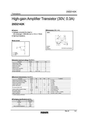
2SD2142K Transistors High-gain Amplifier Transistor (30V, 0.3A) 2SD2142K Dimensions (Unit mm) Features 1) Darlington connection for a high hFE. SMT3 (DC current gain = 5000 (Min.) at VCE = 3V, IC = 10mA) 2.9 1.1 2) High input impedance. 0.4 0.8 (3) Inner circuit (2) (1) C 0.95 0.95 0.15 1.9 (1)Emitter (2)Base B Each lead has same dimensions (3)Collector... See More ⇒
9.7. Size:157K rohm
2sd2143.pdf
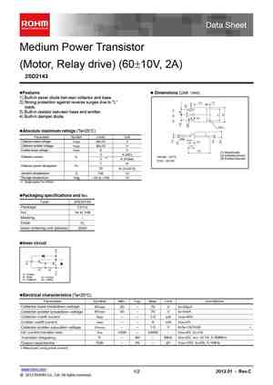
Medium Power Transistor (Motor, Relay drive) (60 10V, 2A) 2SD2143 Features Dimensions (Unit mm) 1) Built-in zener diode between collector and base. 5.5 1.5 2) Strong protection against reverse surges due to "L" loads. 3) Built-in resistor between base and emitter. 4) Built-in damper diode. 0.9 C0.5 Absolute maximum ratings (Ta=25 C) Parameter Symbol Limit... See More ⇒
9.8. Size:71K rohm
2sd1866 2sd2212 2sd2212 2sd2143 2sd1866 2sd2397.pdf
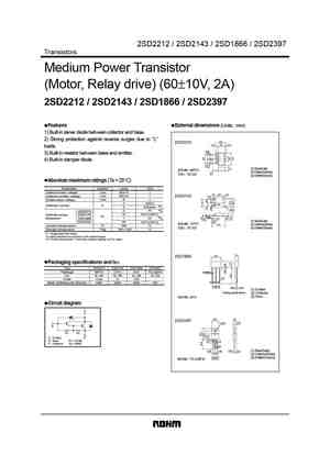
2SD2212 / 2SD2143 / 2SD1866 / 2SD2397 Transistors Medium Power Transistor (Motor, Relay drive) (60 10V, 2A) 2SD2212 / 2SD2143 / 2SD1866 / 2SD2397 Features External dimensions (Units mm) 1) Built-in zener diode between collector and base. 2) Strong protection against reverse surges due to "L" 4.0 2SD2212 1.0 2.5 0.5 loads. (1) 3) Built-in resistor between base and emitter. (2) ... See More ⇒
9.9. Size:177K infineon
bsd214sn.pdf
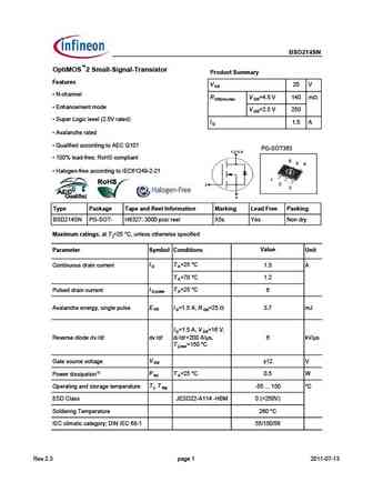
BSD214SN OptiMOS 2 Small-Signal-Transistor Product Summary Features V 20 V DS N-channel R V =4.5 V 140 m DS(on),max GS Enhancement mode V =2.5 V 250 GS Super Logic level (2.5V rated) I 1.5 A D Avalanche rated Qualified according to AEC Q101 PG-SOT363 100% lead-free; RoHS compliant 6 5 4 Halogen-free according to IEC61249-2-21 1 2 3 Type... See More ⇒
9.10. Size:329K secos
2sd2142.pdf
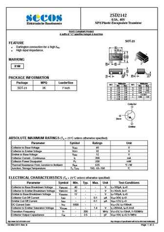
2SD2142 0.3A , 40V NPN Plastic-Encapsulate Transistor Elektronische Bauelemente RoHS Compliant Product A suffix of -C specifies halogen & lead-free SOT-23 FEATURE Darlington connection for a high hFE. A L High input impedance. 3 3 Top View C B MARKING 1 1 2 2 K E R1M D H J F G PACKAGE INFORMATION Package MPQ LeaderSize Millimeter Millimeter REF. R... See More ⇒
9.11. Size:23K sanken-ele
2sd2141.pdf
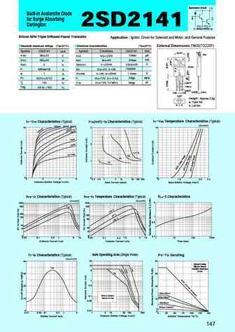
Equivalent circuit C Built-in Avalanche Diode B for Surge Absorbing Darlington 2SD2141 (1.5k )(100 ) E Silicon NPN Triple Diffused Planar Transistor Application Ignitor, Driver for Solenoid and Motor, and General Purpose Absolute maximum ratings (Ta=25 C) Electrical Characteristics (Ta=25 C) External Dimensions FM20(TO220F) Symbol 2SD2141 Symbol Conditions 2SD2141 Unit Un... See More ⇒
9.12. Size:424K htsemi
2sd2142.pdf
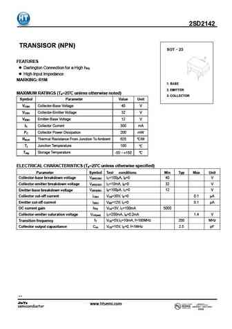
2S 2142 D TRANSISOR (NPN) SOT 23 FEATURES Darlington Connection for a High hFE High Input Impedance MARKING R1M 1. BASE 2. EMITTER MAXIMUM RATINGS (Ta=25 unless otherwise noted) 3. COLLECTOR Symbol Parameter Value Unit VCBO Collector-Base Voltage 40 V VCEO Collector-Emitter Voltage 32 V V Emitter-Base Voltage 12 V EBO I Collector Current 300 mA C ... See More ⇒
9.13. Size:910K kexin
2sd2142.pdf
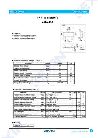
SMD Type Transistors NPN Transistors 2SD2142 SOT-23 Unit mm 2.9+0.1 -0.1 +0.1 0.4 -0.1 3 Features Collector Current Capability IC=300mA 1 2 Collector Emitter Voltage VCEO=32V +0.1 +0.05 0.95 -0.1 0.1 -0.01 1.9+0.1 -0.1 1.Base 2.Emitter 3.collector Absolute Maximum Ratings Ta = 25 Parameter Symbol Rating Unit Collector - Base Voltage VCBO 40 Colle... See More ⇒
9.14. Size:193K inchange semiconductor
2sd214.pdf
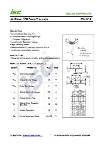
INCHANGE Semiconductor isc Silicon NPN Power Transistor 2SD214 DESCRIPTION Excellent Safe Operating Area Collector-Emitter Sustaining Voltage- V = 100V(Min.) CEO(SUS) Low Collector Saturation Voltage- High Switching Speed Minimum Lot-to-Lot variations for robust device performance and reliable operation APPLICATIONS Designed for high power amplifier and switching appli... See More ⇒
9.15. Size:185K inchange semiconductor
2sd2141.pdf
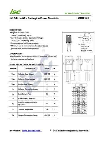
INCHANGE Semiconductor isc Silicon NPN Darlington Power Transistor 2SD2141 DESCRIPTION High DC Current Gain- h = 1500(Min)@ I = 3A FE C Low Collector-Emitter Saturation Voltage- V = 1.5V(Max)@ I = 4A CE(sat) C Incorporating a built-in zener diode Minimum Lot-to-Lot variations for robust device performance and reliable operation APPLICATIONS Designed for use in ignitor... See More ⇒
9.16. Size:190K inchange semiconductor
2sd2148.pdf
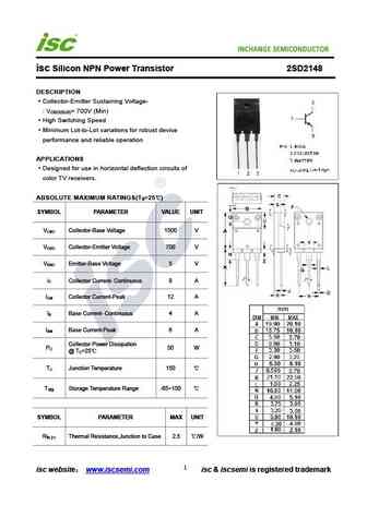
isc Product Specification isc Silicon NPN Power Transistor 2SD2148 DESCRIPTION Collector-Emitter Sustaining Voltage- V = 700V (Min) CEO(SUS) High Switching Speed Minimum Lot-to-Lot variations for robust device performance and reliable operation APPLICATIONS Designed for use in horizontal deflection circuits of color TV receivers. ABSOLUTE MAXIMUM RATINGS(T =25 ) a SYMB... See More ⇒
9.17. Size:202K inchange semiconductor
2sd2140.pdf
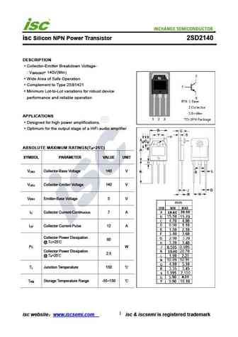
isc Silicon NPN Power Transistor 2SD2140 DESCRIPTION Collector-Emitter Breakdown Voltage- V = 140V(Min) (BR)CEO Wide Area of Safe Operation Complement to Type 2SB1421 Minimum Lot-to-Lot variations for robust device performance and reliable operation APPLICATIONS Designed for high power amplifications. Optimum for the output stage of a HiFi audio amplifier ABSOLUTE MAXI... See More ⇒
9.18. Size:216K inchange semiconductor
2sd2143.pdf
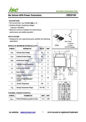
isc Silicon NPN Power Transistors 2SD2143 DESCRIPTION DC Current Gain -h 1000(Min)@ I = 1A FE C Collector-Emitter Sustaining Voltage- V = 60V(Min) CEO(SUS) Minimum Lot-to-Lot variations for robust device performance and reliable operation APPLICATIONS Designed for use in general purpose amplifier and switching applications ABSOLUTE MAXIMUM RATINGS(T =25 ) a SYMBOL PAR... See More ⇒
Detailed specifications: SD202DC
, SD203DC
, SD210
, SD2100
, SD210DE
, SD212
, SD212DE
, SD214
, K3569
, SD217DE
, SD219DE
, SD403BD
, SD403CY
, SD5000N
, SD5001N
, SD5002N
, SD5400CY
.
Keywords - SD214DE MOSFET specs
SD214DE cross reference
SD214DE equivalent finder
SD214DE pdf lookup
SD214DE substitution
SD214DE replacement
Need a MOSFET replacement?
Our guide shows you how to find a perfect substitute by comparing key parameters and specs