IRFS4229PBF Datasheet. Specs and Replacement
Type Designator: IRFS4229PBF 📄📄
Type of Transistor: MOSFET
Type of Control Channel: N-Channel
Absolute Maximum Ratings
Pd ⓘ - Maximum Power Dissipation: 330 W
|Vds|ⓘ - Maximum Drain-Source Voltage: 250 V
|Vgs|ⓘ - Maximum Gate-Source Voltage: 30 V
|Id| ⓘ - Maximum Drain Current: 45 A
Tj ⓘ - Maximum Junction Temperature: 175 °C
Electrical Characteristics
tr ⓘ - Rise Time: 31 nS
Cossⓘ - Output Capacitance: 390 pF
RDSonⓘ - Maximum Drain-Source On-State Resistance: 0.048 Ohm
Package: TO-263
📄📄 Copy
IRFS4229PBF substitution
- MOSFET ⓘ Cross-Reference Search
IRFS4229PBF datasheet
irfs4229pbf.pdf
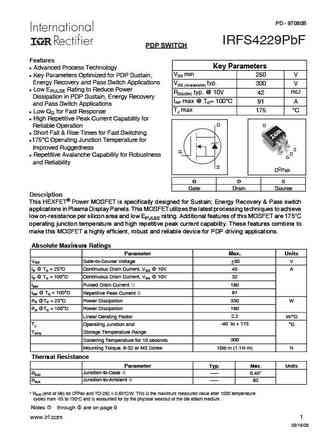
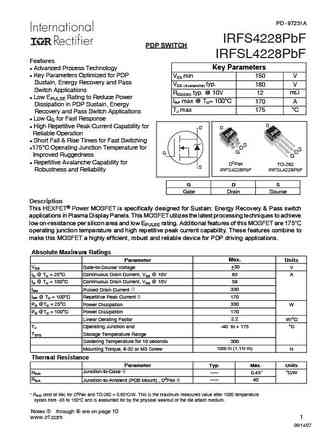
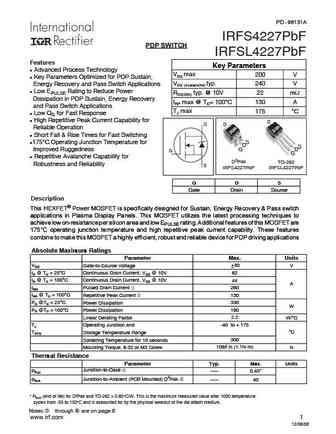
PD - 97080B IRFS4229PbF PDP SWITCH Features Key Parameters l Advanced Process Technology VDS min 250 V l Key Parameters Optimized for PDP Sustain, Energy Recovery and Pass Switch Applications VDS (Avalanche) typ. 300 V l Low EPULSE Rating to Reduce Power RDS(ON) typ. @ 10V m 42 Dissipation in PDP Sustain, Energy Recovery IRP max @ TC= 100 C 91 A and Pass Switch Application... See More ⇒
irfs4229(2).pdf
_0001.jpg)
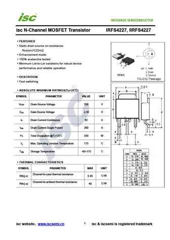
Isc N-Channel MOSFET Transistor IRFS4229 FEATURES With To-263(D2PAK) package Low input capacitance and gate charge Low gate input resistance 100% avalanche tested Minimum Lot-to-Lot variations for robust device performance and reliable operation APPLICATIONS Switching applications ABSOLUTE MAXIMUM RATINGS(T =25 ) a SYMBOL PARAMETER VALUE UNIT V Drain-Source Volt... See More ⇒
irfs4229.pdf
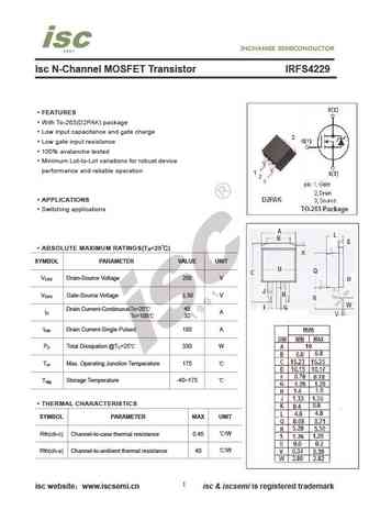
Isc N-Channel MOSFET Transistor IRFS4229 FEATURES With To-263(D2PAK) package Low input capacitance and gate charge Low gate input resistance 100% avalanche tested Minimum Lot-to-Lot variations for robust device performance and reliable operation APPLICATIONS Switching applications ABSOLUTE MAXIMUM RATINGS(T =25 ) a SYMBOL PARAMETER VALUE UNIT V Drain-Source Volt... See More ⇒
irfs4228pbf irfsl4228pbf.pdf
PD - 97231A IRFS4228PbF PDP SWITCH IRFSL4228PbF Features l Advanced Process Technology Key Parameters l Key Parameters Optimized for PDP VDS min 150 V Sustain, Energy Recovery and Pass VDS (Avalanche) typ. 180 V Switch Applications RDS(ON) typ. @ 10V m 12 l Low EPULSE Rating to Reduce Power IRP max @ TC= 100 C 170 A Dissipation in PDP Sustain, Energy TJ max 175 C Reco... See More ⇒
Detailed specifications: IRFS4010PBF, IRFS4020PBF, IRFS4115-7PPBF, IRFS4115PBF, IRFS4127PBF, IRFS41N15DPBF, IRFS4227PBF, IRFS4228PBF, BS170, IRFS4310PBF, IRFS4310ZPBF, IRFS4321-7PPBF, IRFS4321PBF, STB100N10F7, STB100NF03L-03-1, STB100NF03L-03T4, STB100NF04T4
Keywords - IRFS4229PBF MOSFET specs
IRFS4229PBF cross reference
IRFS4229PBF equivalent finder
IRFS4229PBF pdf lookup
IRFS4229PBF substitution
IRFS4229PBF replacement
Can't find your MOSFET? Learn how to find a substitute transistor by analyzing voltage, current and package compatibility
History: MXP6018CD
🌐 : EN ES РУ

LIST
Last Update
MOSFET: CS65N25AKR | AOL1718 | BCD70N07A | BCD90N03 | BCD80N06 | T50N06 | H50N06 | BCD12N65 | BCT12N65 | BCD4N65
Popular searches
2sa940 transistor datasheet | 2sb549 | 5n50 mosfet equivalent | a1016 transistor | a1693 transistor | a933 datasheet | c535 transistor | irf3205 reemplazo