ST1004SRG Specs and Replacement
Type Designator: ST1004SRG
Type of Transistor: MOSFET
Type of Control Channel: N-Channel
Absolute Maximum Ratings
Pd ⓘ - Maximum Power Dissipation: 1.25 W
|Vds|ⓘ - Maximum Drain-Source Voltage: 100 V
|Vgs|ⓘ - Maximum Gate-Source Voltage: 20 V
|Id| ⓘ - Maximum Drain Current: 3 A
Tj ⓘ - Maximum Junction Temperature: 150 °C
Electrical Characteristics
tr ⓘ - Rise Time: 21.5 nS
Cossⓘ - Output Capacitance: 29 pF
RDSonⓘ - Maximum Drain-Source On-State Resistance: 0.31 Ohm
Package: SOT-23
ST1004SRG substitution
- MOSFET ⓘ Cross-Reference Search
ST1004SRG datasheet
st1004srg.pdf
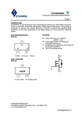
ST1004SRG N Channel Enhancement Mode MOSFET 2.0A DESCRIPTION ST1004SRG is the N-Channel logic enhancement mode power field effect transistor which is produced using high cell density, DMOS trench technology. The process is especially to improve the overall efficiency of DC/DC conventional switching PWM controllers. It has been optimized for low gate charge, low R and fast switchi... See More ⇒
bst100.pdf
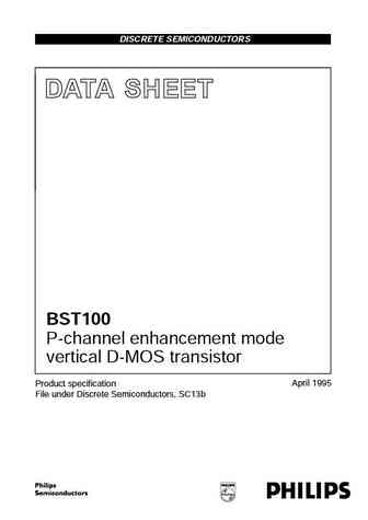
DISCRETE SEMICONDUCTORS DATA SHEET BST100 P-channel enhancement mode vertical D-MOS transistor April 1995 Product specification File under Discrete Semiconductors, SC13b Philips Semiconductors Product specification P-channel enhancement mode vertical BST100 D-MOS transistor DESCRIPTION QUICK REFERENCE DATA P-channel vertical D-MOS transistor Drain-source voltage -VDS max. 60 V T... See More ⇒
st1005srg.pdf
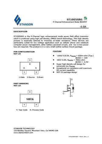
ST1005SRG P Channel Enhancement Mode MOSFET -0.8A DESCRIPTION ST1005SRG is the P-Channel logic enhancement mode power field effect transistor which is produced using high cell density, DMOS trench technology. This high density process is especially tailored to minimize on-state resistance. These devices are particularly suited for low voltage application such as cellular phone an... See More ⇒
st1002.pdf
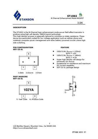
ST1002 N Channel Enhancement Mode MOSFET 3.0A DESCRIPTION The ST1002 is the N-Channel logic enhancement mode power field effect transistor is produce using high cell density, DMOS trench technology. This high-density process is especially tailored to minimize on-state resistance. These device are particularly suited for low voltage application such as cellular phone and notebo... See More ⇒
Detailed specifications: SRM7N65TF-E1, SRM7N65TC-E1, SS05N70, SS07N70, SSD80N03, SSFM2506L, SSFM2508, ST1002, IRF640, ST1005SRG, ST10E4, ST12N10D, ST13P10, ST2300, ST2300SRG, ST2301A, ST2302
Keywords - ST1004SRG MOSFET specs
ST1004SRG cross reference
ST1004SRG equivalent finder
ST1004SRG pdf lookup
ST1004SRG substitution
ST1004SRG replacement
Can't find your MOSFET? Learn how to find a substitute transistor by analyzing voltage, current and package compatibility
