MMBFJ112 Specs and Replacement
Type Designator: MMBFJ112
Type of Transistor: MOSFET
Type of Control Channel: N-Channel
Absolute Maximum Ratings
Pd ⓘ - Maximum Power Dissipation: 0.35 W
|Vds|ⓘ - Maximum Drain-Source Voltage: 35 V
|Id| ⓘ - Maximum Drain Current: 0.005 A
Tj ⓘ - Maximum Junction Temperature: 150 °C
Electrical Characteristics
RDSonⓘ - Maximum Drain-Source On-State Resistance: 50 Ohm
Package: SOT-23
MMBFJ112 substitution
- MOSFET ⓘ Cross-Reference Search
MMBFJ112 datasheet
mmbfj111 mmbfj112 mmbfj113.pdf
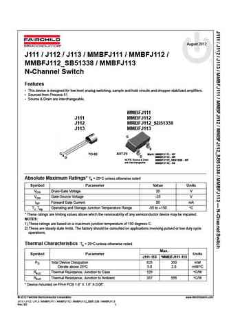
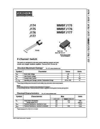
August 2012 J111 / J112 / J113 / MMBFJ111 / MMBFJ112 / MMBFJ112_SB51338 / MMBFJ113 N-Channel Switch Features This device is designed for low level analog switching, sample and hold circuits and chopper stabilized amplifiers. Sourced from Process 51. Source & Drain are interchangeable. MMBFJ111 J111 MMBFJ112 J112 MMBFJ112_SB51338 J113 MMBFJ113 G S SOT-23 G TO-92 Mark... See More ⇒
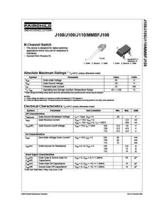
j111 j112 j113 mmbfj111 mmbfj112 mmbfj113.pdf
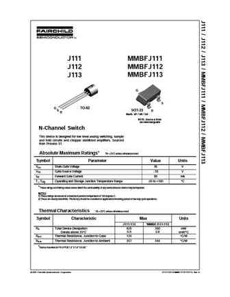
J111 MMBFJ111 J112 MMBFJ112 J113 MMBFJ113 G S G TO-92 S SOT-23 D D Mark 6P / 6R / 6S NOTE Source & Drain are interchangeable N-Channel Switch This device is designed for low level analog switching, sample and hold circuits and chopper stabilized amplifiers. Sourced from Process 51. Absolute Maximum Ratings* TA = 25 C unless otherwise noted Symbol Parameter Value Units VDG D... See More ⇒
mmbfj110.pdf
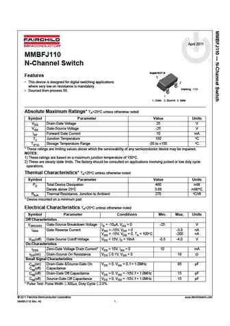
April 2011 MMBFJ110 N-Channel Switch SuperSOT-3 Features 3 This device is designed for digital switching applications 2 where very low on resistance is mandatory. Marking 110 Sourced from process 58. 1 1. Drain 2. Source 3. Gate Absolute Maximum Ratings* TA=25 C unless otherwise noted Symbol Parameter Value Units VDG Drain-Gate Voltage 25 V VGS Gate-Source Voltage -... See More ⇒
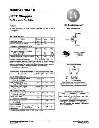
mmbfj175.pdf
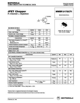
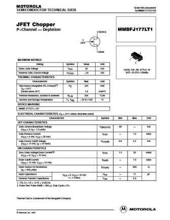
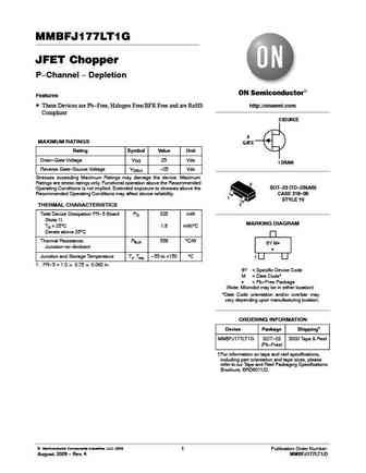
MOTOROLA Order this document SEMICONDUCTOR TECHNICAL DATA by MMBFJ175LT1/D JFET Chopper MMBFJ175LT1 P Channel Depletion Motorola Preferred Device 2 SOURCE 3 GATE 3 1 DRAIN 1 2 MAXIMUM RATINGS Rating Symbol Value Unit CASE 318 08, STYLE 10 SOT 23 (TO 236AB) Drain Gate Voltage VDG 25 V Reverse Gate Source Voltage VGS(r) 25 V THERMAL CHARACTERISTICS Charact... See More ⇒


Detailed specifications: MM20N050P, MM68N06K, MM9N090P, MMBF0202PLT1, MMBF2202PT1, MMBFJ108, MMBFJ110, MMBFJ111, 2SK3568, MMBFJ113, MMBFJ305, MMD50R380PRH, MMD60R360PRH, MMD60R580PRH, MMD60R750PRH, MMD60R900PRH, MMD70R1K4PRH
Keywords - MMBFJ112 MOSFET specs
MMBFJ112 cross reference
MMBFJ112 equivalent finder
MMBFJ112 pdf lookup
MMBFJ112 substitution
MMBFJ112 replacement
Can't find your MOSFET? Learn how to find a substitute transistor by analyzing voltage, current and package compatibility
History: RSJ400N06FRA
🌐 : EN ES РУ

LIST
Last Update
MOSFET: FTF30P35D | FTF25N35DHVT | FTF15N35D | FTE15C35G | FTP02P15G | FTE02P15G | AKF30N5P0SX | AKF30N10S | AKF20P45D | CM4407
Popular searches
fgpf4536 datasheet | p20nm60fp datasheet | 2sc1943 | 7408 mosfet | cs630 | 2sc2705 transistor | 647 transistor | d525 transistor