SM9993DSQG Datasheet. Specs and Replacement
Type Designator: SM9993DSQG 📄📄
Type of Transistor: MOSFET
Type of Control Channel: N-Channel
Absolute Maximum Ratings
Pd ⓘ - Maximum Power Dissipation: 1.56 W
|Vds|ⓘ - Maximum Drain-Source Voltage: 20 V
|Vgs|ⓘ - Maximum Gate-Source Voltage: 12 V
|Id| ⓘ - Maximum Drain Current: 12 A
Tj ⓘ - Maximum Junction Temperature: 150 °C
Electrical Characteristics
tr ⓘ - Rise Time: 10 nS
Cossⓘ - Output Capacitance: 265 pF
RDSonⓘ - Maximum Drain-Source On-State Resistance: 0.0074 Ohm
Package: DFN2X3-6
📄📄 Copy
SM9993DSQG substitution
- MOSFET ⓘ Cross-Reference Search
SM9993DSQG datasheet
sm9993dsqg.pdf
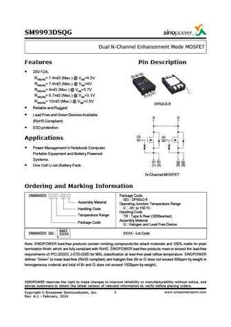
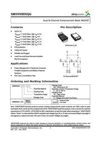
SM9993DSQG Dual N-Channel Enhancement Mode MOSFET Features Pin Description 20V/12A, G2 S2S2 RDS(ON)= 7.4m (Max.) @ VGS=4.5V RDS(ON)= 7.6m (Max.) @ VGS=4V RDS(ON)= 8m (Max.) @ VGS=3.7V G1 RDS(ON)= 8.7m (Max.) @ VGS=3.1V S1S1 RDS(ON)= 10m (Max.) @ VGS=2.5V DFN2x3-6 Reliable and Rugged Lead Free and Green Devices Available D D (RoHS Compliant) ESD protection (3) (4)... See More ⇒
sm9992dsqg.pdf
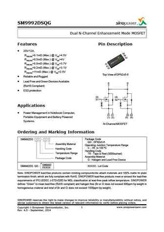
SM9992DSQG Dual N-Channel Enhancement Mode MOSFET Features Pin Description 20V/12A, S2 RDS(ON)=8.1m (Max.) @ VGS=4.5V S2 G2 RDS(ON)=8.5m (Max.) @ VGS=4V RDS(ON)=8.8m (Max.) @ VGS=3.7V S1 S1 RDS(ON)=9.2m (Max.) @ VGS=3.1V G1 RDS(ON)=11m (Max.) @ VGS=2.5V Top View of DFN2x5-6 Reliable and Rugged Lead Free and Green Devices Available D D (RoHS Complian... See More ⇒
sm9990dsqg.pdf
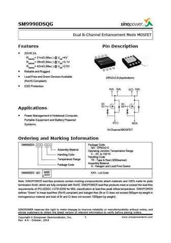
SM9990DSQG Dual N-Channel Enhancement Mode MOSFET Features Pin Description 20V/6.2A, RDS(ON)= 31m (Max.) @ VGS=4V RDS(ON)= 36m (Max.) @ VGS=3.1V RDS(ON)= 42m (Max.) @ VGS=2.5V Reliable and Rugged Lead Free and Green Devices Available DFN2x2-8 (top/bottom) (RoHS Compliant) ESD Protection D(5) D(6) D(7) D(8) (2) (4) G1 G2 Applications Power Management in Notebook Compute... See More ⇒
sm9994dso.pdf
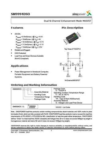
SM9994DSO Dual N-Channel Enhancement Mode MOSFET Features Pin Description D S2 20V/9A, S2 G2 RDS(ON)= 9.5m (max.) @ VGS= 4.5V RDS(ON)= 10m (max.) @ VGS= 4V D S1 RDS(ON)= 10.5m (max.) @ VGS= 3.7V S1 G1 RDS(ON)= 11.5m (max.) @ VGS= 3.1V RDS(ON)= 13m (max.) @ VGS= 2.5V Top View of TSSOP-8 Reliable and Rugged (1) (8) ESD Protected D D Lead Free and Green Devices Available ... See More ⇒
Detailed specifications: SM8A04NSF, SM8A04NSFP, SM8A04NSU, SM8A05NSF, SM8A05NSFP, SM9188DSO, SM9988CO, SM9989DSQG, 60N06, SM9A01NSF, SM9A01NSFP, SMC2333, SMC2342A, SMC2360, SMC3054, SMC3056, SMC3400
Keywords - SM9993DSQG MOSFET specs
SM9993DSQG cross reference
SM9993DSQG equivalent finder
SM9993DSQG pdf lookup
SM9993DSQG substitution
SM9993DSQG replacement
Can't find your MOSFET? Learn how to find a substitute transistor by analyzing voltage, current and package compatibility
MOSFET Parameters. How They Affect Each Other
History: NCE65T1K2K | SVF13N50PN
🌐 : EN ES РУ
LIST
Last Update
MOSFET: CS95118 | CS85105A | CS75N45 | CS72N12 | CS55N50 | CS48N75A | CS40N27 | MSQ60P04D | MSQ40P07D | MSQ30P40D
Popular searches
2n3904 transistor | 2sd424 | 2sc828 | 2n4125 | tip42c transistor | c1815 transistor datasheet | mj15003 | 2sa1015
