HFP13N50U Specs and Replacement
Type Designator: HFP13N50U
Type of Transistor: MOSFET
Type of Control Channel: N-Channel
Absolute Maximum Ratings
Pd ⓘ - Maximum Power Dissipation: 187 W
|Vds|ⓘ - Maximum Drain-Source Voltage: 500 V
|Vgs|ⓘ - Maximum Gate-Source Voltage: 30 V
|Id| ⓘ - Maximum Drain Current: 13 A
Tj ⓘ - Maximum Junction Temperature: 150 °C
Electrical Characteristics
tr ⓘ - Rise Time: 80 nS
Cossⓘ - Output Capacitance: 170 pF
RDSonⓘ - Maximum Drain-Source On-State Resistance: 0.48 Ohm
Package: TO-220
HFP13N50U substitution
- MOSFET ⓘ Cross-Reference Search
HFP13N50U datasheet
hfp13n50u.pdf
Nov 2013 BVDSS = 500 V RDS(on) typ = 0.39 HFP13N50U ID = 13 A 500V N-Channel MOSFET TO-220 FEATURES Originative New Design Superior Avalanche Rugged Technology 1 2 3 Robust Gate Oxide Technology 1.Gate 2. Drain 3. Source Very Low Intrinsic Capacitances Excellent Switching Characteristics Unrivalled Gate Charge 34 nC (Typ.) Extended Safe Operating Area Low... See More ⇒
hfp13n50.pdf
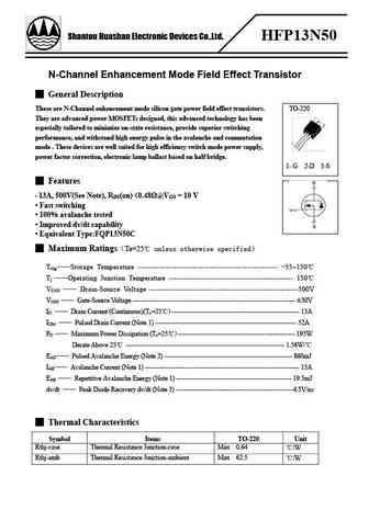
Shantou Huashan Electronic Devices Co.,Ltd. HFP13N50 N-Channel Enhancement Mode Field Effect Transistor General Description These are N-Channel enhancement mode silicon gate power field effect transistors. TO-220 They are advanced power MOSFETs designed, this advanced technology has been especially tailored to minimize on-state resistance, provide superior switching performan... See More ⇒
hfp13n50s.pdf
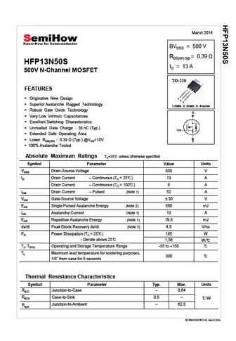
March 2014 BVDSS = 500 V RDS(on) typ HFP13N50S ID = 13 A 500V N-Channel MOSFET TO-220 FEATURES Originative New Design 1 2 3 Superior Avalanche Rugged Technology 1.Gate 2. Drain 3. Source Robust Gate Oxide Technology Very Low Intrinsic Capacitances Excellent Switching Characteristics Unrivalled Gate Charge 38 nC (Typ.) Extended Safe Operating Area L... See More ⇒
hfp13n10.pdf
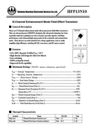
Shantou Huashan Electronic Devices Co.,Ltd. HFP13N10 N-Channel Enhancement Mode Field Effect Transistor General Description These are N-Channel enhancement mode silicon gate power field effect transistors. TO-220 They are advanced power MOSFETs designed, this advanced technology has been especially tailored to minimize on-state resistance, provide superior switching performan... See More ⇒
Detailed specifications: HFP10N65U, HFP10N80, HFP11N40, HFP12N60S, HFP12N60U, HFP12N65S, HFP12N65U, HFP13N50S, IRF1404, HFP13N60U, HFP13N65U, HFP18N50U, HFP2N60S, HFP2N60U, HFP2N65S, HFP2N65U, HFP2N70S
Keywords - HFP13N50U MOSFET specs
HFP13N50U cross reference
HFP13N50U equivalent finder
HFP13N50U pdf lookup
HFP13N50U substitution
HFP13N50U replacement
Step-by-step guide to finding a MOSFET replacement. Cross-reference parts and ensure compatibility for your repair or project.
🌐 : EN ES РУ
LIST
Last Update
MOSFET: CM4407 | CM3407 | CM3400 | SVF11N65F | SVF11N65T | FKBB3105 | EHBA036R1 | CRTT067N10N | AP6NA3R2MT | AP65SA145DDT8
Popular searches
c2166 transistor | 2sd330 | 20n60 | ksa1013 | mje15032g datasheet | 2sc2166 | 2sc5198 | 2sc1971


