HFW11N40 Specs and Replacement
Type Designator: HFW11N40
Type of Transistor: MOSFET
Type of Control Channel: N-Channel
Absolute Maximum Ratings
Pd ⓘ - Maximum Power Dissipation: 147 W
|Vds|ⓘ - Maximum Drain-Source Voltage: 400 V
|Vgs|ⓘ - Maximum Gate-Source Voltage: 30 V
|Id| ⓘ - Maximum Drain Current: 11.4 A
Tj ⓘ - Maximum Junction Temperature: 150 °C
Electrical Characteristics
tr ⓘ - Rise Time: 120 nS
Cossⓘ - Output Capacitance: 180 pF
RDSonⓘ - Maximum Drain-Source On-State Resistance: 0.48 Ohm
Package: D2-PAK
HFW11N40 substitution
- MOSFET ⓘ Cross-Reference Search
HFW11N40 datasheet
hfw11n40.pdf
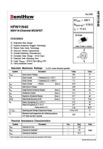
Dec 2005 BVDSS = 400 V RDS(on) typ HFW11N40 ID = 11.4 A 400V N-Channel MOSFET D2-PAK FEATURES Originative New Design Superior Avalanche Rugged Technology 1.Gate 2. Drain 3. Source Robust Gate Oxide Technology Very Low Intrinsic Capacitances Excellent Switching Characteristics Unrivalled Gate Charge 35 nC (Typ.) Extended Safe Operating Area Lower RDS(ON) ... See More ⇒
Detailed specifications: HFS8N65U, HFS8N70S, HFS8N70U, HFS8N80, HFS9N50, HFT1N60S, HFU630, HFW10N60S, IRF3205, HFW12N60S, HFW50N06, HFW5N50S, HFW5N60S, HFW5N65S, HFW5N65U, HFW640, HFW6N90
Keywords - HFW11N40 MOSFET specs
HFW11N40 cross reference
HFW11N40 equivalent finder
HFW11N40 pdf lookup
HFW11N40 substitution
HFW11N40 replacement
Need a MOSFET replacement? Our guide shows you how to find a perfect substitute by comparing key parameters and specs
