MTP3055E Specs and Replacement
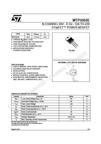
Type Designator: MTP3055E
Type of Transistor: MOSFET
Type of Control Channel: N-Channel
Absolute Maximum Ratings
Pd ⓘ - Maximum Power Dissipation: 70 W
|Vds|ⓘ - Maximum Drain-Source Voltage: 60 V
|Vgs|ⓘ - Maximum Gate-Source Voltage: 20 V
|Id| ⓘ - Maximum Drain Current: 14 A
Tj ⓘ - Maximum Junction Temperature: 175 °C
Electrical Characteristics
Cossⓘ - Output Capacitance: 450 pF
RDSonⓘ - Maximum Drain-Source On-State Resistance: 0.15 Ohm
Package: TO220
MTP3055E substitution
- MOSFET ⓘ Cross-Reference Search
MTP3055E datasheet
mtp3055e.pdf
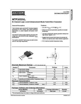
MTP3055E N-CHANNEL 60V - 0.1 - 12ATO-220 STripFET POWER MOSFET TYPE VDSS RDS(on) ID MTP3055E 60 V ... See More ⇒
mtp3055vlrev2a.pdf
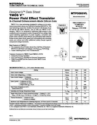
MOTOROLA Order this document SEMICONDUCTOR TECHNICAL DATA by MTP3055VL/D Designer's Data Sheet MTP3055VL TMOS V Motorola Preferred Device Power Field Effect Transistor N Channel Enhancement Mode Silicon Gate TMOS POWER FET TMOS V is a new technology designed to achieve an on resis- 12 AMPERES tance area product about one half that of standard MOSFETs. This 60 VOLTS ... See More ⇒
mtp3055vl.pdf
MOTOROLA Order this document SEMICONDUCTOR TECHNICAL DATA by MTP3055VL/D Designer's Data Sheet MTP3055VL TMOS V Motorola Preferred Device Power Field Effect Transistor N Channel Enhancement Mode Silicon Gate TMOS POWER FET TMOS V is a new technology designed to achieve an on resis- 12 AMPERES tance area product about one half that of standard MOSFETs. This 60 VOLTS ... See More ⇒
mtp3055vrev2a.pdf
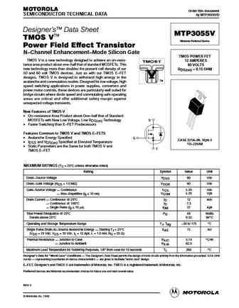
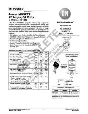
MOTOROLA Order this document SEMICONDUCTOR TECHNICAL DATA by MTP3055V/D Designer's Data Sheet MTP3055V TMOS V Motorola Preferred Device Power Field Effect Transistor N Channel Enhancement Mode Silicon Gate TMOS POWER FET TMOS V is a new technology designed to achieve an on resis- 12 AMPERES tance area product about one half that of standard MOSFETs. This 60 VOLTS... See More ⇒
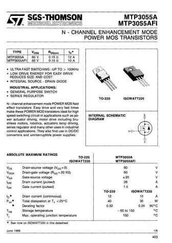
Detailed specifications: MNT-LB32N16, MNT-LB32N16-C4, MNT-LB32N20, MNT-LB32N20-C4, MTB30N06VL, MTB30P06V, MTB35N06ZL, MTP10N10M, 18N50, MTP3055EFI, MTP30N05E, MTP30N08M, MTP3N50E, MTP3N60, MTP3N60FI, MTP6N60, NDB4050
Keywords - MTP3055E MOSFET specs
MTP3055E cross reference
MTP3055E equivalent finder
MTP3055E pdf lookup
MTP3055E substitution
MTP3055E replacement
Learn how to find the right MOSFET substitute. A guide to cross-reference, check specs and replace MOSFETs in your circuits.
🌐 : EN ES РУ
LIST
Last Update
MOSFET: AUB062N08BG | AUB060N08AG | AUB056N10 | AUB056N08BGL | AUB050N085 | AUB050N055 | AUB045N12 | AUB045N10BT | AUB039N10 | AUB034N10
Popular searches
2sc5242 | irf540 equivalent | mp1620 transistor equivalent | 2sc945 transistor | c2073 transistor | ac176 transistor | mpsa20 | irfp264
