TSM3911DCX6 Specs and Replacement
Type Designator: TSM3911DCX6
Type of Transistor: MOSFET
Type of Control Channel: P-Channel
Absolute Maximum Ratings
Pd ⓘ - Maximum Power Dissipation: 1.15 W
|Vds|ⓘ - Maximum Drain-Source Voltage: 20 V
|Vgs|ⓘ - Maximum Gate-Source Voltage: 8 V
|Id| ⓘ - Maximum Drain Current: 2.2 A
Tj ⓘ - Maximum Junction Temperature: 150 °C
Electrical Characteristics
tr ⓘ - Rise Time: 3.73 nS
Cossⓘ - Output Capacitance: 145.54 pF
RDSonⓘ - Maximum Drain-Source On-State Resistance: 0.14 Ohm
Package: SOT-26
TSM3911DCX6 substitution
- MOSFET ⓘ Cross-Reference Search
TSM3911DCX6 datasheet
tsm3911dcx6.pdf
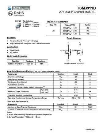
TSM3911D 20V Dual P-Channel MOSFET SOT-26 Pin Definition PRODUCT SUMMARY 1. Gate 1 6. Drain 1 2. Source 2 5, Source 1 VDS (V) RDS(on)(m ) ID (A) 3. Gate 2 4. Drain 2 140 @ VGS = -4.5V -2.2 -20 200 @ VGS = -2.5V -1.8 300 @ VGS = -1.8V -1.5 Features Block Diagram Advance Trench Process Technology High Density Cell Design for Ultra Low On-resistance Applica... See More ⇒
tsm3900dcx6.pdf
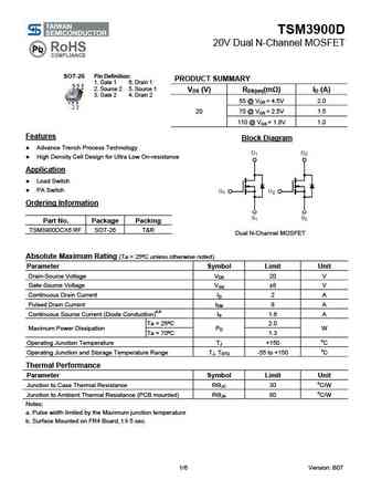
TSM3900D 20V Dual N-Channel MOSFET SOT-26 Pin Definition PRODUCT SUMMARY 1. Gate 1 6. Drain 1 2. Source 2 5. Source 1 VDS (V) RDS(on)(m ) ID (A) 3. Gate 2 4. Drain 2 55 @ VGS = 4.5V 2.0 20 70 @ VGS = 2.5V 1.5 110 @ VGS = 1.8V 1.0 Features Block Diagram Advance Trench Process Technology High Density Cell Design for Ultra Low On-resistance Application ... See More ⇒
Detailed specifications: TSM3460CX6, TSM3462CX6, TSM3481CX6, TSM3548DCX6, TSM35N03CP, TSM35N03PQ56, TSM35N10CP, TSM3900DCX6, 4435, TSM3N80CH, TSM3N80CI, TSM3N80CP, TSM3N80CZ, TSM3N90CH, TSM3N90CI, TSM3N90CP, TSM3N90CZ
Keywords - TSM3911DCX6 MOSFET specs
TSM3911DCX6 cross reference
TSM3911DCX6 equivalent finder
TSM3911DCX6 pdf lookup
TSM3911DCX6 substitution
TSM3911DCX6 replacement
Step-by-step guide to finding a MOSFET replacement. Cross-reference parts and ensure compatibility for your repair or project.
🌐 : EN ES РУ

LIST
Last Update
MOSFET: AUP060N055 | AUP056N10 | AUP056N08BGL | AUP052N085 | AUP045N12 | AUP039N10 | AUP034N10 | AUP034N06 | AUP033N08BG | AUP026N085
Popular searches
tip117 | 2n3643 | 2sc2078 transistor equivalent | 2sc2073 | a608 transistor | c536 transistor | 2n706 | 2n388