TSM9434DCS Datasheet. Specs and Replacement
Type Designator: TSM9434DCS 📄📄
Type of Transistor: MOSFET
Type of Control Channel: P-Channel
Absolute Maximum Ratings
Pd ⓘ - Maximum Power Dissipation: 2.5 W
|Vds|ⓘ - Maximum Drain-Source Voltage: 20 V
|Vgs|ⓘ - Maximum Gate-Source Voltage: 8 V
|Id| ⓘ - Maximum Drain Current: 6.4 A
Tj ⓘ - Maximum Junction Temperature: 150 °C
Electrical Characteristics
tr ⓘ - Rise Time: 43 nS
Cossⓘ - Output Capacitance: 191 pF
RDSonⓘ - Maximum Drain-Source On-State Resistance: 0.04 Ohm
Package: SOP-8
📄📄 Copy
TSM9434DCS substitution
- MOSFET ⓘ Cross-Reference Search
TSM9434DCS datasheet
tsm9434dcs.pdf
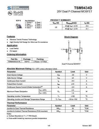
TSM9434D 20V Dual P-Channel MOSFET PRODUCT SUMMARY SOP-8 Pin Definition 1. Source 1 8. Drain 1 VDS (V) RDS(on)(m ) ID (A) 2. Gate 1 7. Drain 1 3. Source 2 6. Drain 2 40 @ VGS = -4.5V -6.4 -20 4. Gate 2 5. Drain 2 60 @ VGS = -2.5V -5.1 Features Block Diagram Advance Trench Process Technology High Density Cell Design for Ultra Low On-resistance Appli... See More ⇒
tsm9434cs.pdf
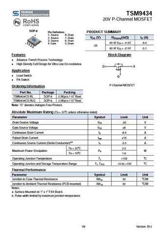
TSM9434 20V P-Channel MOSFET SOP-8 Pin Definition PRODUCT SUMMARY 1. Source 8. Drain 2. Source 7. Drain VDS (V) RDS(on)(m ) ID (A) 3. Source 6. Drain 40 @ VGS = -4.5V -6.4 4. Gate 5. Drain -20 60 @ VGS = -2.5V -5.1 Features Block Diagram Advance Trench Process Technology High Density Cell Design for Ultra Low On-resistance Application Load Switch ... See More ⇒
tsm9435cs.pdf

TSM9435 30V P-Channel MOSFET SOP-8 Pin Definition PRODUCT SUMMARY 1. Source 2. Source VDS (V) RDS(on)(m ) ID (A) 3. Source 60 @ VGS = 10V -5.3 4. Gate -30 5, 6, 7, 8. Drain 90 @ VGS = 4.5V -4.2 Features Block Diagram Advance Trench Process Technology High Density Cell Design for Ultra Low On-resistance Application Load Switch PA Swit... See More ⇒
tsm9428dcs.pdf
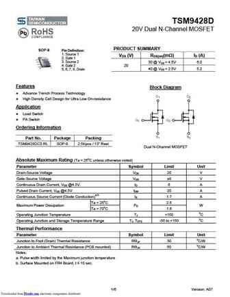
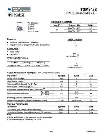
TSM9428D 20V Dual N-Channel MOSFET PRODUCT SUMMARY SOP-8 Pin Definition 1. Source 1 VDS (V) RDS(on)(m ) ID (A) 2. Gate 1 3. Source 2 30 @ VGS = 4.5V 6.0 4. Gate 2 20 40 @ VGS = 2.5V 5.2 5, 6, 7, 8. Drain Features Block Diagram Advance Trench Process Technology High Density Cell Design for Ultra Low On-resistance Application Load Switch P... See More ⇒
Detailed specifications: TSM8N70CI, TSM8N80CI, TSM8N80CZ, TSM9409CS, TSM9426DCS, TSM9428CS, TSM9428DCS, TSM9434CS, AON7408, TSM9435CS, TSM9926DCS, TSM9933DCS, TSM9966DCX6, TSM9N50CI, TSM9N50CZ, TSM9N90CI, TSM9N90CN
Keywords - TSM9434DCS MOSFET specs
TSM9434DCS cross reference
TSM9434DCS equivalent finder
TSM9434DCS pdf lookup
TSM9434DCS substitution
TSM9434DCS replacement
Need a MOSFET replacement? Our guide shows you how to find a perfect substitute by comparing key parameters and specs
