BUK455-100B Datasheet. Specs and Replacement
Type Designator: BUK455-100B 📄📄
Type of Transistor: MOSFET
Type of Control Channel: N-Channel
Absolute Maximum Ratings
Pd ⓘ - Maximum Power Dissipation: 125 W
|Vds|ⓘ - Maximum Drain-Source Voltage: 100 V
|Vgs|ⓘ - Maximum Gate-Source Voltage: 30 V
|Id| ⓘ - Maximum Drain Current: 23 A
Tj ⓘ - Maximum Junction Temperature: 175 °C
Electrical Characteristics
tr ⓘ - Rise Time: 25 nS
Cossⓘ - Output Capacitance: 350 pF
RDSonⓘ - Maximum Drain-Source On-State Resistance: 0.1 Ohm
Package: TO-220AB
📄📄 Copy
BUK455-100B substitution
- MOSFET ⓘ Cross-Reference Search
BUK455-100B datasheet
buk455-100b.pdf

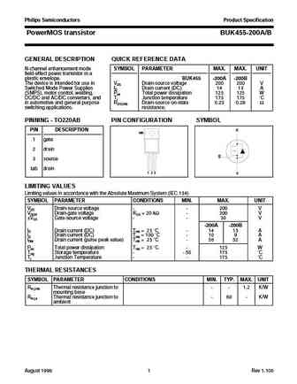
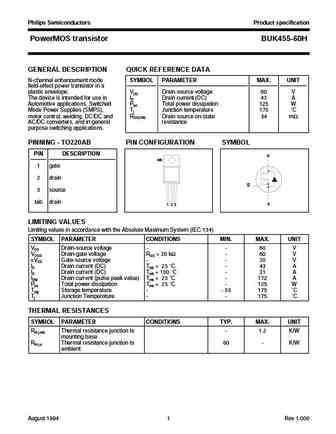
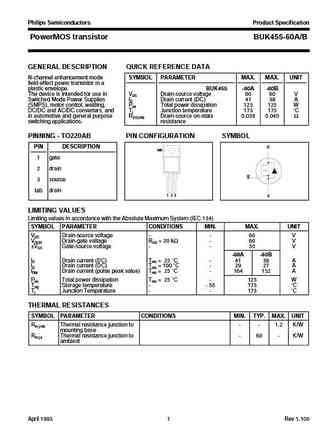
Philips Semiconductors Product Specification PowerMOS transistor BUK455-100A/B GENERAL DESCRIPTION QUICK REFERENCE DATA N-channel enhancement mode SYMBOL PARAMETER MAX. MAX. UNIT field-effect power transistor in a plastic envelope. BUK455 -100A -100B The device is intended for use in VDS Drain-source voltage 100 100 V Switched Mode Power Supplies ID Drain current (DC) 26 23 A (SMPS), ... See More ⇒
buk455-100a-b 1.pdf

Philips Semiconductors Product Specification PowerMOS transistor BUK455-100A/B GENERAL DESCRIPTION QUICK REFERENCE DATA N-channel enhancement mode SYMBOL PARAMETER MAX. MAX. UNIT field-effect power transistor in a plastic envelope. BUK455 -100A -100B The device is intended for use in VDS Drain-source voltage 100 100 V Switched Mode Power Supplies ID Drain current (DC) 26 23 A (SMPS), ... See More ⇒
buk455-100.pdf
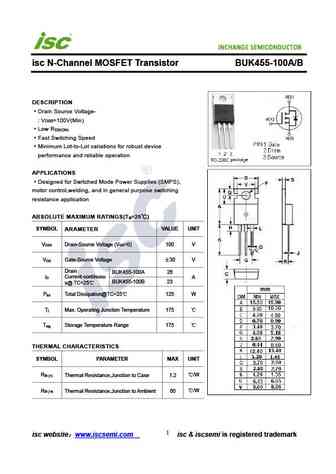
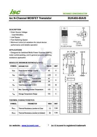
isc N-Channel MOSFET Transistor BUK455-100A/B DESCRIPTION Drain Source Voltage- V =100V(Min) DSS Low R DS(ON) Fast Switching Speed Minimum Lot-to-Lot variations for robust device performance and reliable operation APPLICATIONS Designed for Switched Mode Power Supplies (SMPS), motor control,welding, and in general purpose switching resistance application ABSOLUTE MAXIMU... See More ⇒
buk455-200a-b 1.pdf
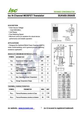
Philips Semiconductors Product Specification PowerMOS transistor BUK455-200A/B GENERAL DESCRIPTION QUICK REFERENCE DATA N-channel enhancement mode SYMBOL PARAMETER MAX. MAX. UNIT field-effect power transistor in a plastic envelope. BUK455 -200A -200B The device is intended for use in VDS Drain-source voltage 200 200 V Switched Mode Power Supplies ID Drain current (DC) 14 13 A (SMPS), ... See More ⇒


Detailed specifications: BUK127-50DL, BUK127-50GT, BUK128-50DL, BUK129-50DL, BUK138-50DL, BUK139-50DL, BUK1M200-50SGTD, BUK452-100B, STF13NM60N, BUK455-200B, BUK456-100B, BUK472-100A, BUK472-100B, BUK543-100B, BUK553-100B, BUK553-60A, BUK553-60B
Keywords - BUK455-100B MOSFET specs
BUK455-100B cross reference
BUK455-100B equivalent finder
BUK455-100B pdf lookup
BUK455-100B substitution
BUK455-100B replacement
Can't find your MOSFET? Learn how to find a substitute transistor by analyzing voltage, current and package compatibility
MOSFET Parameters. How They Affect Each Other
History: HM3710
🌐 : EN ES РУ

LIST
Last Update
MOSFET: CEZC2P07 | CEZ2R05 | CEU3133 | CES2361 | CES2312A | CEP100N10L | CEM3425 | CEM3139 | CEM3133 | CEM3115
Popular searches
hy3210 | d313 transistor equivalent | 2sb827 | c5200 datasheet | 2n2614 | 2sa777 replacement | 2sc828 transistor | 2sd357