CS2N60I Specs and Replacement
Type Designator: CS2N60I
Type of Transistor: MOSFET
Type of Control Channel: N-Channel
Absolute Maximum Ratings
Pd ⓘ
- Maximum Power Dissipation: 45 W
|Vds|ⓘ - Maximum Drain-Source Voltage: 600 V
|Vgs|ⓘ - Maximum Gate-Source Voltage: 30 V
|Id| ⓘ - Maximum Drain Current: 2 A
Tj ⓘ - Maximum Junction Temperature: 150 °C
Electrical Characteristics
tr ⓘ - Rise Time: 23 nS
Cossⓘ -
Output Capacitance: 35 pF
RDSonⓘ - Maximum Drain-Source On-State Resistance: 5 Ohm
Package: TO-251
- MOSFET ⓘ Cross-Reference Search
CS2N60I datasheet
..1. Size:269K foshan
cs2n60i.pdf 

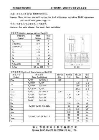
BRI2N60(CS2N60I) N-CHANNEL MOSFET/N MOS DC/DC Purpose These devices are well suited for high efficiency switching DC/DC converters and switch mode power supplies. , , Features Low gate charge, low crss, fast switching. /Absolute maximum ratings(Ta=25 ... See More ⇒
8.1. Size:373K no
cs2n60-f.pdf 

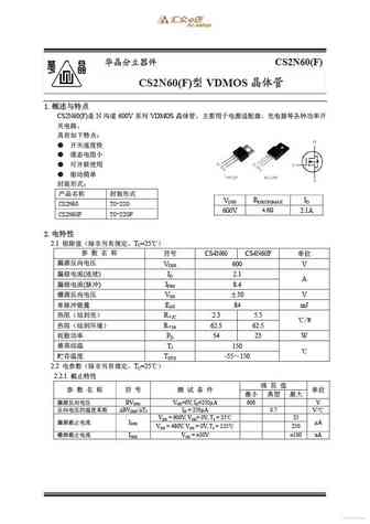
CS2N60(F) CS2N60(F) VDMOS 1. CS2N60(F) N 600V VDMOS VDSS RDS(ON)MAX ID CS2N60 TO-220 ... See More ⇒
8.3. Size:1813K jilin sino
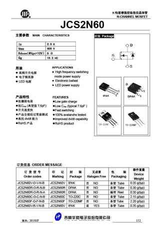
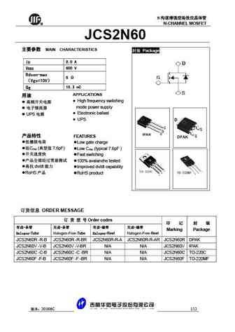
jcs2n60t jcs2n60v jcs2n60r jcs2n60c jcs2n60f.pdf 

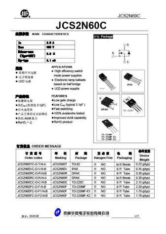
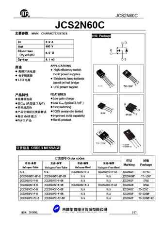
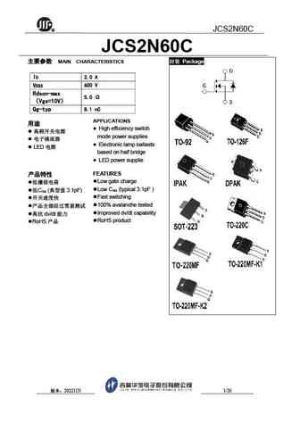
R JCS2N60C JCS2N60C MAIN CHARACTERISTICS Package ID 2.0 A VDSS 600 V Rdson-max 5.0 Vgs=10V Qg-typ 8.1 nC APPLICATIONS l High efficiency switch l mode power supplies l l Electronic lamp ballasts l LED based on half bridge l LED power supplie FEATURES l Low gate c... See More ⇒
8.9. Size:153K can-sheng
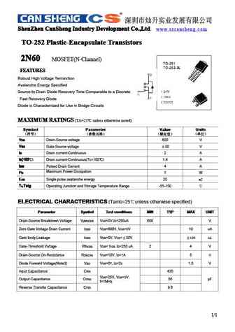
cs2n60 to-252.pdf 

ShenZhen CanSheng Industry Development Co.,Ltd ShenZhen CanSheng Industry Development Co.,Ltd ShenZhen CanSheng Industry Development Co.,Ltd www.szcansheng.com ShenZhen CanSheng Industry Development Co.,Ltd. TO-252 Plastic-Encapsulate Transistors TO-252 Plastic-Encapsulate Transistors TO-252 Plastic-Encapsulate Transistors TO-252 Plastic-Encapsula... See More ⇒
8.10. Size:334K crhj
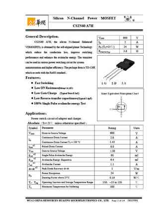
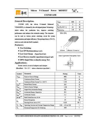
cs2n60 a7h.pdf 

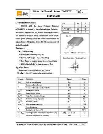
Silicon N-Channel Power MOSFET R CS2N60 A7H General Description VDSS 600 V CS2N60 A7H, the silicon N-channel Enhanced ID 2 A PD (TC=25 ) 24 W VDMOSFETs, is obtained by the self-aligned planar Technology RDS(ON)Typ 3.6 which reduce the conduction loss, improve switching performance and enhance the avalanche energy. The transistor can be used in various power... See More ⇒
8.11. Size:334K crhj
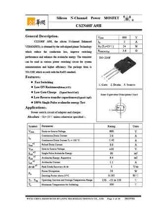
cs2n60f a9h.pdf 

Silicon N-Channel Power MOSFET R CS2N60F A9H General Description VDSS 600 V CS2N60F A9H, the silicon N-channel Enhanced ID 2 A PD (TC=25 ) 24 W VDMOSFETs, is obtained by the self-aligned planar Technology RDS(ON)Typ 3.6 which reduce the conduction loss, improve switching performance and enhance the avalanche energy. The transistor can be used in various pow... See More ⇒
8.12. Size:357K crhj
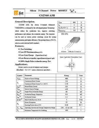
cs2n60 a3h.pdf 

Silicon N-Channel Power MOSFET R CS2N60 A3H General Description VDSS 600 V CS2N60 A3H, the silicon N-channel Enhanced ID 2 A PD (TC=25 ) 35 W VDMOSFETs, is obtained by the self-aligned planar Technology RDS(ON)Typ 3.6 which reduce the conduction loss, improve switching performance and enhance the avalanche energy. The transistor can be used in various power ... See More ⇒
8.13. Size:355K crhj
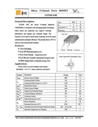
cs2n60 a4h.pdf 

Silicon N-Channel Power MOSFET R CS2N60 A4H General Description VDSS 600 V CS2N60 A4H, the silicon N-channel Enhanced ID 2 A PD (TC=25 ) 35 W VDMOSFETs, is obtained by the self-aligned planar Technology RDS(ON)Typ 3.6 which reduce the conduction loss, improve switching performance and enhance the avalanche energy. The transistor can be used in various power... See More ⇒
8.14. Size:356K crhj
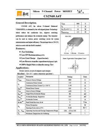
cs2n60 a4t.pdf 

Silicon N-Channel Power MOSFET R CS2N60 A4T General Description VDSS 600 V CS2N60 A4T, the silicon N-channel Enhanced ID 2 A PD (TC=25 ) 35 W VDMOSFETs, is obtained by the self-aligned planar Technology RDS(ON)Typ 3.5 which reduce the conduction loss, improve switching performance and enhance the avalanche energy. The transistor can be used in various power... See More ⇒
8.15. Size:225K wuxi china
cs2n60fa9h.pdf 

Silicon N-Channel Power MOSFET R CS2N60F A9H General Description VDSS 600 V CS2N60F A9H, the silicon N-channel Enhanced ID 2 A PD (TC=25 ) 24 W VDMOSFETs, is obtained by the self-aligned planar Technology RDS(ON)Typ 3.6 which reduce the conduction loss, improve switching performance and enhance the avalanche energy. The transistor can be used in various pow... See More ⇒
8.16. Size:334K wuxi china
cs2n60a7h.pdf 

Silicon N-Channel Power MOSFET R CS2N60 A7H General Description VDSS 600 V CS2N60 A7H, the silicon N-channel Enhanced ID 2 A PD (TC=25 ) 24 W VDMOSFETs, is obtained by the self-aligned planar Technology RDS(ON)Typ 3.6 which reduce the conduction loss, improve switching performance and enhance the avalanche energy. The transistor can be used in various power... See More ⇒
8.17. Size:234K wuxi china
cs2n60a3h.pdf 

Silicon N-Channel Power MOSFET R CS2N60 A3H General Description VDSS 600 V CS2N60 A3H, the silicon N-channel Enhanced ID 2 A PD (TC=25 ) 35 W VDMOSFETs, is obtained by the self-aligned planar Technology RDS(ON)Typ 3.6 which reduce the conduction loss, improve switching performance and enhance the avalanche energy. The transistor can be used in various power... See More ⇒
8.18. Size:356K wuxi china
cs2n60a4t.pdf 

Silicon N-Channel Power MOSFET R CS2N60 A4T General Description VDSS 600 V CS2N60 A4T, the silicon N-channel Enhanced ID 2 A PD (TC=25 ) 35 W VDMOSFETs, is obtained by the self-aligned planar Technology RDS(ON)Typ 3.5 which reduce the conduction loss, improve switching performance and enhance the avalanche energy. The transistor can be used in various power... See More ⇒
8.19. Size:239K wuxi china
cs2n60a4h.pdf 

Silicon N-Channel Power MOSFET R CS2N60 A4H General Description VDSS 600 V CS2N60 A4H, the silicon N-channel Enhanced ID 2 A PD (TC=25 ) 35 W VDMOSFETs, is obtained by the self-aligned planar Technology RDS(ON)Typ 3.6 which reduce the conduction loss, improve switching performance and enhance the avalanche energy. The transistor can be used in various power... See More ⇒
8.20. Size:470K convert
cs2n60f cs2n60p cs2n60u cs2n60d cs2n60c.pdf 

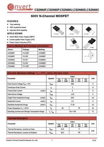
nvert Suzhou Convert Semiconductor Co ., Ltd. CS2N60F,CS2N60P,CS2N60U,CS2N60D,CS2N60C 600V N-Channel MOSFET FEATURES Fast switching 100% avalanche tested Improved dv/dt capability APPLICATIONS Switch Mode Power Supply (SMPS) Uninterruptible Power Supply (UPS) Power Factor Correction (PFC) Device Marking and Package Information Device Package Marking CS2N60F... See More ⇒
8.21. Size:201K inchange semiconductor
jcs2n60f.pdf 
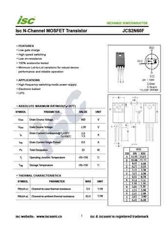
INCHANGE Semiconductor Isc N-Channel MOSFET Transistor JCS2N60F FEATURES Low gate charge High speed switching Low on-resistance 100% avalanche tested Minimum Lot-to-Lot variations for robust device performance and reliable operation APPLICATIONS High frequency switching mode power supply Electronic ballast UPS ABSOLUTE MAXIMUM RATINGS(T =25 ) a SYMBOL PARA... See More ⇒
Detailed specifications: CS2837AND, CS2907Z, CS2N50A4, CS2N60A3H, CS2N60A4H, CS2N60A4T, CS2N60A7H, CS2N60FA9H, AON7408, CS2N65A3, CS2N65A3HY, CS2N65A4HY, CS2N65FA9HY, CS2N70A3R, CS2N70A4, CS2N70A6, CS2N70FA9
Keywords - CS2N60I MOSFET specs
CS2N60I cross reference
CS2N60I equivalent finder
CS2N60I pdf lookup
CS2N60I substitution
CS2N60I replacement
Need a MOSFET replacement?
Our guide shows you how to find a perfect substitute by comparing key parameters and specs
